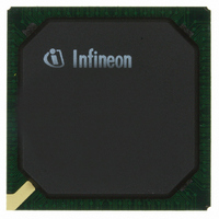
PXB4220E-V32 Infineon Technologies, PXB4220E-V32 Datasheet - Page 41

PXB4220E-V32
Manufacturer Part Number
PXB4220E-V32
Description
IC CHIPSET 8 E1/T1 LINE 256-BGA
Manufacturer
Infineon Technologies
Datasheet
1.PXB4220E-V33.pdf
(290 pages)
Specifications of PXB4220E-V32
Applications
*
Interface
*
Voltage - Supply
*
Package / Case
256-BGA
Mounting Type
Surface Mount
Lead Free Status / RoHS Status
Contains lead / RoHS non-compliant
Other names
PXB4220E-V32
PXB4220E-V32IN
PXB4220E-V32IN
Available stocks
Company
Part Number
Manufacturer
Quantity
Price
Company:
Part Number:
PXB4220E-V32
Manufacturer:
Infineon
Quantity:
35
Company:
Part Number:
PXB4220E-V32
Manufacturer:
Infineon Technologies
Quantity:
10 000
- Current page: 41 of 290
- Download datasheet (4Mb)
Table 11
Block
CV
RB
CK
JT
ICRC
External
RAM
Data Sheet
Functions
External Clock Recovery interface
• Generation of serial communication frames to external clock recovery
• Generation of synchronization for RTS generation by external clock
• Reception of frames with RTS values from external clock recovery circuit
RTS Buffer
• Buffer for 2 incoming RTS values per port
Clock & Reset
• Clock distribution
• Reset control
JTAG interface
• Boundary Scan register
• TAP controller
Internal Clock Recovery Circuit
• Synchronous Residual Time Stamp SRTS
• Adaptive Clock Method ACM
ATM Transmit Buffer
• Compensate packetization delay on the PDH interface.
• Maximum size of 256 ATM cells per port.
• Maximum size of 64 octets per ATM cell.
ATM Receive Buffer
• Maximum size of 16 ATM cells per port.
• Maximum size of 64 octets per ATM cell.
Segmentation Buffer
• Compensate segmentation delay in the ATM network.
• 1024 bytes per port (unstructured CES)
• 256 bytes per timeslot (structured CES)
Reassembly Buffer
• Compensate the Cell Delay Variation (CDV) of the ATM network.
• 512 bytes per timeslot. (structured CES)
Functions of IWE8 Blocks (cont’d)
circuit, containing RTS values and or ACM buffer filling
recovery circuit.
41
PXB 4219E, PXB 4220E, PXB 4221E
Functional Description
IWE8, V3.4
2003-01-20
Related parts for PXB4220E-V32
Image
Part Number
Description
Manufacturer
Datasheet
Request
R

Part Number:
Description:
IC CHIPSET 8 E1/T1 LINE 256-BGA
Manufacturer:
Infineon Technologies
Datasheet:

Part Number:
Description:
Interworking Element for 8 E1/T1 Lines
Manufacturer:
Infineon Technologies AG
Datasheet:

Part Number:
Description:
members of Infineon ATM Chipset
Manufacturer:
Infineon Technologies AG
Datasheet:

Part Number:
Description:
Manufacturer:
Infineon Technologies AG
Datasheet:

Part Number:
Description:
Manufacturer:
Infineon Technologies AG
Datasheet:

Part Number:
Description:
Manufacturer:
Infineon Technologies AG
Datasheet:

Part Number:
Description:
Manufacturer:
Infineon Technologies AG
Datasheet:

Part Number:
Description:
Manufacturer:
Infineon Technologies AG
Datasheet:

Part Number:
Description:
Manufacturer:
Infineon Technologies AG
Datasheet:

Part Number:
Description:
Manufacturer:
Infineon Technologies AG
Datasheet:

Part Number:
Description:
16-bit microcontroller with 2x2 KByte RAM
Manufacturer:
Infineon Technologies AG
Datasheet:

Part Number:
Description:
NPN silicon RF transistor
Manufacturer:
Infineon Technologies AG
Datasheet:

Part Number:
Description:
NPN silicon RF transistor
Manufacturer:
Infineon Technologies AG
Datasheet:

Part Number:
Description:
NPN silicon RF transistor
Manufacturer:
Infineon Technologies AG
Datasheet:

Part Number:
Description:
NPN silicon RF transistor
Manufacturer:
Infineon Technologies AG
Datasheet:


