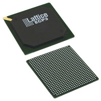
LFE3-35EA-8FN672I Lattice, LFE3-35EA-8FN672I Datasheet - Page 15

LFE3-35EA-8FN672I
Manufacturer Part Number
LFE3-35EA-8FN672I
Description
IC FPGA 33.3K LUTS 310I/O FN672
Manufacturer
Lattice
Series
ECP3r
Datasheets
1.LFE3-150EA-7FN672C.pdf
(136 pages)
2.LFE3-35EA-8FN672I.pdf
(4 pages)
3.LFE3-35EA-8FN672I.pdf
(21 pages)
Specifications of LFE3-35EA-8FN672I
Number Of Logic Elements/cells
33000
Number Of Labs/clbs
4125
Total Ram Bits
1358848
Number Of I /o
310
Number Of Gates
-
Voltage - Supply
1.14 V ~ 1.26 V
Mounting Type
Surface Mount
Operating Temperature
-40°C ~ 100°C
Package / Case
672-BBGA
Lead Free Status / Rohs Status
Lead free / RoHS Compliant
Other names
220-1163
- LFE3-150EA-7FN672C PDF datasheet
- LFE3-35EA-8FN672I PDF datasheet #2
- LFE3-35EA-8FN672I PDF datasheet #3
- Current page: 15 of 136
- Download datasheet (3Mb)
Lattice Semiconductor
Figure 2-10. Primary Clock Sources for LatticeECP3-35
Figure 2-11. Primary Clock Sources for LatticeECP3-70, -95, -150
DLL Input
PLL Input
PLL Input
PLL Input
PLL Input
DLL Input
PLL Input
PLL Input
PLL Input
Clock
Clock
Clock
Clock
Input
Input
Input
Input
Note: Clock inputs can be configured in differential or single-ended mode.
Note: Clock inputs can be configured in differential or single-ended mode.
DLL
PLL
DLL
PLL
PLL
PLL
PLL
CLK
PLL
PLL
CLK
DIV
DIV
From Routing
From Routing
Clock Input
to Eight Quadrant Clock Selection
Clock Input
to Eight Quadrant Clock Selection
SERDES
Primary Clock Sources
Primary Clock Sources
Quad
Clock Input
Clock Input
SERDES
2-12
Quad
SERDES
SERDES
Quad
Quad
From Routing
From Routing
(ECP3-150 only)
SERDES
Quad
LatticeECP3 Family Data Sheet
CLK
DLL
CLK
DLL
DIV
PLL
PLL
DIV
PLL
PLL
PLL
PLL
PLL
PLL Input
Clock
Input
Clock
Input
DLL Input
PLL Input
PLL Input
PLL Input
Clock
Input
Clock
Input
DLL Input
PLL Input
PLL Input
PLL Input
Architecture
Related parts for LFE3-35EA-8FN672I
Image
Part Number
Description
Manufacturer
Datasheet
Request
R
Part Number:
Description:
33.3K LUTS, 295 I/O, 1.2V, -6 SPEED, PB-FREE
Manufacturer:
LATTICE SEMICONDUCTOR
Datasheet:
Part Number:
Description:
FPGA LatticeECP3™ Family 33000 Cells 65nm Technology 1.2V 484-Pin FBGA
Manufacturer:
LATTICE SEMICONDUCTOR
Datasheet:

Part Number:
Description:
IC FPGA 33.3KLUTS 133I/O 256BGA
Manufacturer:
Lattice
Datasheet:

Part Number:
Description:
IC FPGA 33.3KLUTS 133I/O 256BGA
Manufacturer:
Lattice
Datasheet:

Part Number:
Description:
IC FPGA 33.3KLUTS 295I/O 484BGA
Manufacturer:
Lattice
Datasheet:

Part Number:
Description:
IC FPGA 33.3KLUTS 310I/O 672BGA
Manufacturer:
Lattice
Datasheet:

Part Number:
Description:
IC FPGA 33.3KLUTS 310I/O 672BGA
Manufacturer:
Lattice
Datasheet:

Part Number:
Description:
IC FPGA 35KLUTS 133I/O 256-BGA
Manufacturer:
Lattice
Datasheet:

Part Number:
Description:
IC FPGA 35KLUTS 133I/O 256-BGA
Manufacturer:
Lattice
Datasheet:

Part Number:
Description:
IC FPGA 33KLUTS 295I/O 484-BGA
Manufacturer:
Lattice
Datasheet:

Part Number:
Description:
IC FPGA 33KLUTS 295I/O 484-BGA
Manufacturer:
Lattice
Datasheet:

Part Number:
Description:
IC FPGA 35KLUTS 133I/O 256-BGA
Manufacturer:
Lattice
Datasheet:

Part Number:
Description:
IC FPGA 33KLUTS 295I/O 484-BGA
Manufacturer:
Lattice
Datasheet:

Part Number:
Description:
IC FPGA 33.3KLUTS 672FPBGA
Manufacturer:
Lattice
Datasheet:

Part Number:
Description:
IC FPGA 33.3KLUTS 256FTBGA
Manufacturer:
Lattice
Datasheet:


