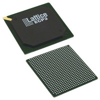
LFE3-35EA-8FN672I Lattice, LFE3-35EA-8FN672I Datasheet - Page 42

LFE3-35EA-8FN672I
Manufacturer Part Number
LFE3-35EA-8FN672I
Description
IC FPGA 33.3K LUTS 310I/O FN672
Manufacturer
Lattice
Series
ECP3r
Datasheets
1.LFE3-150EA-7FN672C.pdf
(136 pages)
2.LFE3-35EA-8FN672I.pdf
(4 pages)
3.LFE3-35EA-8FN672I.pdf
(21 pages)
Specifications of LFE3-35EA-8FN672I
Number Of Logic Elements/cells
33000
Number Of Labs/clbs
4125
Total Ram Bits
1358848
Number Of I /o
310
Number Of Gates
-
Voltage - Supply
1.14 V ~ 1.26 V
Mounting Type
Surface Mount
Operating Temperature
-40°C ~ 100°C
Package / Case
672-BBGA
Lead Free Status / Rohs Status
Lead free / RoHS Compliant
Other names
220-1163
- LFE3-150EA-7FN672C PDF datasheet
- LFE3-35EA-8FN672I PDF datasheet #2
- LFE3-35EA-8FN672I PDF datasheet #3
- Current page: 42 of 136
- Download datasheet (3Mb)
Lattice Semiconductor
Figure 2-37. DQS Local Bus
Polarity Control Logic
In a typical DDR Memory interface design, the phase relationship between the incoming delayed DQS strobe and
the internal system clock (during the READ cycle) is unknown. The LatticeECP3 family contains dedicated circuits
to transfer data between these domains. A clock polarity selector is used to prevent set-up and hold violations at
the domain transfer between DQS (delayed) and the system clock. This changes the edge on which the data is reg-
istered in the synchronizing registers in the input register block. This requires evaluation at the start of each READ
cycle for the correct clock polarity.
Prior to the READ operation in DDR memories, DQS is in tristate (pulled by termination). The DDR memory device
drives DQS low at the start of the preamble state. A dedicated circuit detects the first DQS rising edge after the pre-
amble state. This signal is used to control the polarity of the clock to the synchronizing registers.
DDR3 Memory Support
LatticeECP3 supports the read and write leveling required for DDR3 memory interfaces.
Read leveling is supported by the use of the DDRCLKPOL and the DDRLAT signals generated in the DQS Read
Control logic block. These signals dynamically control the capture of the data with respect to the DQS at the input
register block.
Data Output Register Block
DQS Output Register Block
Data Input Register Block
DQS Write Control Logic
DQS Read Control Logic
DQS Delay Block
DDR DLL
2-39
LatticeECP3 Family Data Sheet
DDR Data
Pad
DQS
Pad
Architecture
Related parts for LFE3-35EA-8FN672I
Image
Part Number
Description
Manufacturer
Datasheet
Request
R
Part Number:
Description:
33.3K LUTS, 295 I/O, 1.2V, -6 SPEED, PB-FREE
Manufacturer:
LATTICE SEMICONDUCTOR
Datasheet:
Part Number:
Description:
FPGA LatticeECP3™ Family 33000 Cells 65nm Technology 1.2V 484-Pin FBGA
Manufacturer:
LATTICE SEMICONDUCTOR
Datasheet:

Part Number:
Description:
IC FPGA 33.3KLUTS 133I/O 256BGA
Manufacturer:
Lattice
Datasheet:

Part Number:
Description:
IC FPGA 33.3KLUTS 133I/O 256BGA
Manufacturer:
Lattice
Datasheet:

Part Number:
Description:
IC FPGA 33.3KLUTS 295I/O 484BGA
Manufacturer:
Lattice
Datasheet:

Part Number:
Description:
IC FPGA 33.3KLUTS 310I/O 672BGA
Manufacturer:
Lattice
Datasheet:

Part Number:
Description:
IC FPGA 33.3KLUTS 310I/O 672BGA
Manufacturer:
Lattice
Datasheet:

Part Number:
Description:
IC FPGA 35KLUTS 133I/O 256-BGA
Manufacturer:
Lattice
Datasheet:

Part Number:
Description:
IC FPGA 35KLUTS 133I/O 256-BGA
Manufacturer:
Lattice
Datasheet:

Part Number:
Description:
IC FPGA 33KLUTS 295I/O 484-BGA
Manufacturer:
Lattice
Datasheet:

Part Number:
Description:
IC FPGA 33KLUTS 295I/O 484-BGA
Manufacturer:
Lattice
Datasheet:

Part Number:
Description:
IC FPGA 35KLUTS 133I/O 256-BGA
Manufacturer:
Lattice
Datasheet:

Part Number:
Description:
IC FPGA 33KLUTS 295I/O 484-BGA
Manufacturer:
Lattice
Datasheet:

Part Number:
Description:
IC FPGA 33.3KLUTS 672FPBGA
Manufacturer:
Lattice
Datasheet:

Part Number:
Description:
IC FPGA 33.3KLUTS 256FTBGA
Manufacturer:
Lattice
Datasheet:


