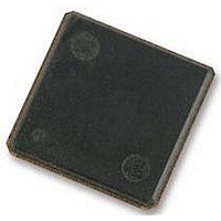
H5TQ2G63BFR-H9C HYNIX SEMICONDUCTOR, H5TQ2G63BFR-H9C Datasheet - Page 57

H5TQ2G63BFR-H9C
Manufacturer Part Number
H5TQ2G63BFR-H9C
Description
58T1898
Manufacturer
HYNIX SEMICONDUCTOR
Datasheet
1.H5TQ2G63BFR-H9C.pdf
(93 pages)
Specifications of H5TQ2G63BFR-H9C
Memory Type
SDRAM
Memory Configuration
128M X 16
Access Time
13.5ns
Interface Type
CMOS
Memory Case Style
FBGA
No. Of Pins
96
Operating Temperature Range
0°C To +85°C
Memory Size
2 Gbit
Rohs Compliant
Yes
Available stocks
Company
Part Number
Manufacturer
Quantity
Price
Company:
Part Number:
H5TQ2G63BFR-H9C
Manufacturer:
AD
Quantity:
1 001
Company:
Part Number:
H5TQ2G63BFR-H9C
Manufacturer:
HYNIX
Quantity:
9 500
Company:
Part Number:
H5TQ2G63BFR-H9C
Manufacturer:
HYNIX
Quantity:
4 000
Part Number:
H5TQ2G63BFR-H9C
Manufacturer:
HYNIX
Quantity:
20 000
Rev. 0.5 / Aug. 2010
(optional)
(optional)
I
I
I
DDQ2NT
I
I
I
I
I
DDQ4R
DD2NT
DD2P0
DD2P1
DD2Q
DD3N
DD3P
Precharge Standby ODT Current
CKE: High; External clock: On; tCK, CL: see Table 1 on page 39; BL: 8
Address, Bank Address Inputs: partially toggling according to Table 6 on page 44; Data IO: FLOATING; DM:
stable at 0; Bank Activity: all banks closed; Output Buffer and RTT: Enabled in Mode Registers
toggling according to Table 6 on page 44; Pattern Details: see Table 6 on page 44
Precharge Standby ODT IDDQ Current
Same definition like for IDD2NT, however measuring IDDQ current instead of IDD current
Precharge Power-Down Current Slow Exit
CKE: Low; External clock: On; tCK, CL: see Table 1 on page 39; BL: 8
Address, Bank Address Inputs: stable at 0; Data IO: FLOATING; DM: stable at 0; Bank Activity: all banks
closed; Output Buffer and RTT: Enabled in Mode Registers
Mode: Slow Exit
Precharge Power-Down Current Fast Exit
CKE: Low; External clock: On; tCK, CL: see Table 1 on page 39; BL: 8
Address, Bank Address Inputs: stable at 0; Data IO: FLOATING; DM: stable at 0; Bank Activity: all banks
closed; Output Buffer and RTT: Enabled in Mode Registers
Mode: Fast Exit
Precharge Quiet Standby Current
CKE: High; External clock: On; tCK, CL: see Table 1 on page 39; BL: 8
Address, Bank Address Inputs: stable at 0; Data IO: FLOATING; DM: stable at 0; Bank Activity: all banks
closed; Output Buffer and RTT: Enabled in Mode Registers
Active Standby Current
CKE: High; External clock: On; tCK, CL: see Table 1 on page 39; BL: 8
Address, Bank Address Inputs: partially toggling according to Table 5 on page 44; Data IO: FLOATING; DM:
stable at 0; Bank Activity: all banks open; Output Buffer and RTT: Enabled in Mode Registers
stable at 0; Pattern Details: see Table 5 on page 44
Active Power-Down Current
CKE: Low; External clock: On; tCK, CL: see Table 1 on page 39; BL: 8
Address, Bank Address Inputs: stable at 0; Data IO: FLOATING; DM: stable at 0; Bank Activity: all banks open;
Output Buffer and RTT: Enabled in Mode Registers
Operating Burst Read IDDQ Current
Same definition like for IDD4R, however measuring IDDQ current instead of IDD current
c)
c)
b)
; ODT Signal: stable at 0
b)
b)
b)
; ODT Signal: stable at 0; Precharge Power Down
; ODT Signal: stable at 0; Precharge Power Down
; ODT Signal: stable at 0
a)
a)
a)
a)
a)
a)
; AL: 0; CS: stable at 1; Command,
; AL: 0; CS: stable at 1; Command,
; AL: 0; CS: stable at 1; Command,
; AL: 0; CS: stable at 1; Command,
; AL: 0; CS: stable at 1; Command,
; AL: 0; CS: stable at 1; Command,
H5TQ2G63BFR
b)
b)
; ODT Signal:
; ODT Signal:
57


