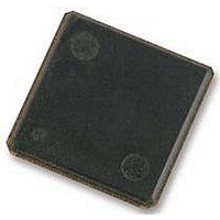
H5TQ2G63BFR-H9C HYNIX SEMICONDUCTOR, H5TQ2G63BFR-H9C Datasheet - Page 80

H5TQ2G63BFR-H9C
Manufacturer Part Number
H5TQ2G63BFR-H9C
Description
58T1898
Manufacturer
HYNIX SEMICONDUCTOR
Datasheet
1.H5TQ2G63BFR-H9C.pdf
(93 pages)
Specifications of H5TQ2G63BFR-H9C
Memory Type
SDRAM
Memory Configuration
128M X 16
Access Time
13.5ns
Interface Type
CMOS
Memory Case Style
FBGA
No. Of Pins
96
Operating Temperature Range
0°C To +85°C
Memory Size
2 Gbit
Rohs Compliant
Yes
Available stocks
Company
Part Number
Manufacturer
Quantity
Price
Company:
Part Number:
H5TQ2G63BFR-H9C
Manufacturer:
AD
Quantity:
1 001
Company:
Part Number:
H5TQ2G63BFR-H9C
Manufacturer:
HYNIX
Quantity:
9 500
Company:
Part Number:
H5TQ2G63BFR-H9C
Manufacturer:
HYNIX
Quantity:
4 000
Part Number:
H5TQ2G63BFR-H9C
Manufacturer:
HYNIX
Quantity:
20 000
Rev. 0.5 / Aug. 2010
22. n = from 13 cycles to 50 cycles.
23. tCH (abs) is the absolute instantaneous clock high pulse width, as measured from one rising edge to the following fall
24. tCL (abs) is the absolute instantaneous clock low pulse width, as measured from one falling edge to the following ris
25. The tIS (base) AC150 specifications are adjusted from the tIS (base) specification by adding an additional 100 ps of
Address / Command Setup, Hold and Derating
For all input signals the total tIS (setup time) and tIH (hold time) required is calculated by adding the data sheet tIS (base)
and tIH (base) value (see Table 11) to the ΔtIS and ΔtIH derating value (see Table 12) respectively. Example: tIS (total
setup time) = tIS (base) + ΔtIS
Setup (tIS) nominal slew rate for a rising signal is defined as the slew rate between the last crossing of V
first crossing of V
crossing of V
line between shaded ‘V
later than the nominal slew rate line anywhere between shaded ‘V
actual signal from the ac level to dc level is used for derating value (see Figure 6).
Hold (tIH) nominal slew rate for a rising signal is defined as the slew rate between the last crossing of Vil (dc) max and the
first crossing of V
ing of Vih (dc) min and the first crossing of V
between shaded ‘dc to V
lier than the nominal slew rate line anywhere between shaded ‘dc to V
actual signal from the dc level to V
For a valid transition the input signal has to remain above/below V
15 mV / sec, then the interval between ZQCS commands is calculated as:
voltage sensitivities. For example, if TSens = 1.5% /
ing edge.
where TSens = max (dRTTdT, dRONdTM) and VSens = max (dRTTdV, dRONdVM) define the SDRAM temperature and
ing edge.
derating to accommodate for the lower alternate threshold of 150 mV and another 25 ps to account for the earlier
reference point [(175 mV - 150 mV) / 1 V/ns].
REF(dc)
REF(dc)
IH(ac)
and the first crossing of Vil (ac) max. If the actual signal is always earlier than the nominal slew rate
min. Setup (tIS) nominal slew rate for a falling signal is defined as the slew rate between the last
REF(dc)
----------------------------------------------------------------------------------------------------------- -
(Tsens x Tdriftrate)+( VSens x Vdriftrate)
----------------------------------------------------- -
(1.5 x 1)+(0.15 x 15)
. Hold (tIH) nominal slew rate for a falling signal is defined as the slew rate between the last cross-
REF(dc)
to ac region’, use nominal slew rate for derating value (see Figure 4). If the actual signal is
region’, use nominal slew rate for derating value (see Figure 5). If the actual signal is ear-
REF(dc)
0.5
level is used for derating value (see Figure 6).
REF(dc)
ZQCorrection
. If the actual signal is always later than the nominal slew rate line
o
C, VSens = 0.15% / mV, Tdriftrate = 1
=
0.133
REF(dc)
IH/IL(ac)
REF(dc)
=
to ac region’, the slew rate of a tangent line to the
for some time t
128ms
region’, the slew rate of a tangent line to the
VAC
(see Table 14).
o
C / sec and Vdriftrate =
H5TQ2G63BFR
REF(dc)
and the
80


