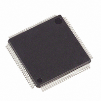
DS21552L+ Maxim Integrated Products, DS21552L+ Datasheet - Page 39

DS21552L+
Manufacturer Part Number
DS21552L+
Description
IC TXRX T1 1-CHIP 5V 100-LQFP
Manufacturer
Maxim Integrated Products
Datasheet
1.DS21352L.pdf
(137 pages)
Specifications of DS21552L+
Function
Single-Chip Transceiver
Interface
E1, HDLC, J1, T1
Number Of Circuits
1
Voltage - Supply
4.75 V ~ 5.25 V
Current - Supply
75mA
Operating Temperature
0°C ~ 70°C
Mounting Type
Surface Mount
Package / Case
100-LQFP
Includes
DSX-1 and CSU Line Build-Out Generator, HDLC Controller, In-Band Loop Code Generator and Detector
Product
Framer
Number Of Transceivers
1
Data Rate
64 Kbps
Supply Voltage (max)
3.465 V
Supply Voltage (min)
3.135 V
Supply Current (max)
75 mA (Typ)
Maximum Operating Temperature
+ 70 C
Minimum Operating Temperature
0 C
Mounting Style
SMD/SMT
Ic Interface Type
Parallel, Serial
Supply Voltage Range
4.75V To 5.25V
Operating Temperature Range
0°C To +70°C
Digital Ic Case Style
LQFP
No. Of Pins
100
Filter Terminals
SMD
Rohs Compliant
Yes
Lead Free Status / RoHS Status
Lead free / RoHS Compliant
Power (watts)
-
Lead Free Status / Rohs Status
Lead free / RoHS Compliant
CCR4: COMMON CONTROL REGISTER 4 (Address=11 Hex)
SYMBOL
(MSB)
RSRE
RFSA1
RPCSI
TPCSI
TIRFS
RSRE
THSE
RFE
RFF
RPCSI
POSITION
CCR4.7
CCR4.6
CCR4.5
CCR4.4
CCR4.3
CCR4.2
CCR4.1
CCR4.0
RFSA1
NAME AND DESCRIPTION
Receive Side Signaling Re–Insertion Enable. See Section 10.2 for details.
0 = do not re–insert signaling bits into the data stream presented at the RSER pin
1 = reinsert the signaling bits into data stream presented at the RSER pin
Receive Per–Channel Signaling Insert. See Section 10.2 for more details.
0 = do not use RCHBLK to determine which channels should have signaling re–inserted
1 = use RCHBLK to determine which channels should have signaling re–inserted
Receive Force Signaling All Ones. See Section 10.2 for more details.
0 = do not force extracted robbed–bit signaling bit positions to a one
1 = force extracted robbed–bit signaling bit positions to a one
Receive Freeze Enable. See Section 10.2 for details.
0 = no freezing of receive signaling data will occur
1 = allow freezing of receive signaling data at RSIG (and RSER if CCR4.7 = 1).
Receive Force Freeze. Freezes receive side signaling at RSIG (and RSER if
CCR4.7=1); will override Receive Freeze Enable (RFE). See Section 10.2 for details.
0 = do not force a freeze event
1 = force a freeze event
Transmit Hardware Signaling Insertion Enable. See Section 10.2 for details.
0 = do not insert signaling from the TSIG pin into the data stream presented at the
TSER pin
1 = insert signaling from the TSIG pin into data stream presented at the TSER pin
Transmit Per–Channel Signaling Insert. See Section 10.2 for details.
0 = do not use TCHBLK to determine which channels should have signaling inserted
from TSIG
1 = use TCHBLK to determine which channels should have signaling inserted from
TSIG
Transmit Idle Registers (TIR) Function Select. See Section 2.1 for timing details.
0 = TIRs define in which channels to insert idle code
1 = TIRs define in which channels to insert data from RSER (i.e., Per-Channel
Loopback function)
RFE
39 of 137
RFF
THSE
TPCSI
TIRFS
(LSB)


