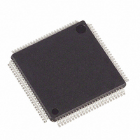
DS21552L+ Maxim Integrated Products, DS21552L+ Datasheet - Page 60

DS21552L+
Manufacturer Part Number
DS21552L+
Description
IC TXRX T1 1-CHIP 5V 100-LQFP
Manufacturer
Maxim Integrated Products
Datasheet
1.DS21352L.pdf
(137 pages)
Specifications of DS21552L+
Function
Single-Chip Transceiver
Interface
E1, HDLC, J1, T1
Number Of Circuits
1
Voltage - Supply
4.75 V ~ 5.25 V
Current - Supply
75mA
Operating Temperature
0°C ~ 70°C
Mounting Type
Surface Mount
Package / Case
100-LQFP
Includes
DSX-1 and CSU Line Build-Out Generator, HDLC Controller, In-Band Loop Code Generator and Detector
Product
Framer
Number Of Transceivers
1
Data Rate
64 Kbps
Supply Voltage (max)
3.465 V
Supply Voltage (min)
3.135 V
Supply Current (max)
75 mA (Typ)
Maximum Operating Temperature
+ 70 C
Minimum Operating Temperature
0 C
Mounting Style
SMD/SMT
Ic Interface Type
Parallel, Serial
Supply Voltage Range
4.75V To 5.25V
Operating Temperature Range
0°C To +70°C
Digital Ic Case Style
LQFP
No. Of Pins
100
Filter Terminals
SMD
Rohs Compliant
Yes
Lead Free Status / RoHS Status
Lead free / RoHS Compliant
Power (watts)
-
Lead Free Status / Rohs Status
Lead free / RoHS Compliant
11.1 TRANSMIT SIDE CODE GENERATION
In the transmit direction there are two methods by which channel data from the backplane can be
overwritten with data generated by the framer. The first method which is covered in Section 11.1 was a
feature contained in the original DS2151 while the second method which is covered in Section 11.2 is a
new feature of the DS2152/352/552.
11.1.1 FIXED PER-CHANNEL IDLE CODE INSERTION
The first method involves using the Transmit Idle Registers (TIR1/2/3) to determine which of the 24 T1
channels should be overwritten with the code placed in the Transmit Idle Definition Register (TIDR).
This method allows the same 8–bit code to be placed into any of the 24 T1 channels. If this method is
used, then the CCR4.0 control bit must be set to zero.
Each of the bit position in the Transmit Idle Registers (TIR1/TIR2/TIR3) represent a DS0 channel in the
outgoing frame. When these bits are set to a one, the corresponding channel will transmit the Idle Code
contained in the Transmit Idle Definition Register (TIDR). Robbed bit signaling and Bit 7 stuffing will
occur over the programmed Idle Code unless the DS0 channel is made transparent by the Transmit
Transparency Registers.
TIR1/TIR2/TIR3: TRANSMIT IDLE REGISTERS (Address=3C to 3E Hex
[Also used for Per–Channel Loopback]
NOTE:
If CCR4.0=1, then a zero in the TIRs implies that channel data is to be sourced from TSER and a one
implies that channel data is to be sourced from the output of the receive side framer (i.e., Per–Channel
Loopback; see Figure 3-1.
TIDR: TRANSMIT IDLE DEFINITION REGISTER (Address=3F Hex)
11.1.2 UNIQUE PER-CHANNEL IDLE CODE INSERTION
The second method involves using the Transmit Channel Control Registers (TCC1/2/3) to determine which of the 24 T1
channels should be overwritten with the code placed in the Transmit Channel Registers (TC1 to TC24). This method is more
flexible than the first in that it allows a different 8–bit code to be placed into each of the 24 T1 channels.
(MSB)
SYMBOLS
CH16
CH24
(MSB)
TIDR7
SYMBOL
CH8
CH1-24
TIDR7
TIDR0
CH15
CH23
CH7
TIDR6
POSITION
POSITIONS
TIDR.7
TIDR.0
TIR1.0-3.7
CH14
CH22
CH6
TIDR5
NAME AND DESCRIPTION
MSB of the Idle Code (this bit is transmitted first)
LSB of the Idle Code (this bit is transmitted last)
CH13
CH21
CH5
NAME AND DESCRIPTION
Transmit Idle Code Insertion Control Bits.
0 = do not insert the Idle Code in the TIDR into this channel
1 = insert the Idle Code in the TIDR into this channel
TIDR4
CH12
CH20
CH4
TIDR3
60 of 137
CH11
CH19
CH3
TIDR2
CH10
CH18
CH2
TIDR1
(LSB)
CH17
CH1
CH9
TIR1 (3C)
TIR2 (3D)
TIR3 (3E)
TIDR0
(LSB)
)


