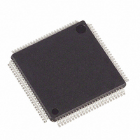
DS21552L+ Maxim Integrated Products, DS21552L+ Datasheet - Page 66

DS21552L+
Manufacturer Part Number
DS21552L+
Description
IC TXRX T1 1-CHIP 5V 100-LQFP
Manufacturer
Maxim Integrated Products
Datasheet
1.DS21352L.pdf
(137 pages)
Specifications of DS21552L+
Function
Single-Chip Transceiver
Interface
E1, HDLC, J1, T1
Number Of Circuits
1
Voltage - Supply
4.75 V ~ 5.25 V
Current - Supply
75mA
Operating Temperature
0°C ~ 70°C
Mounting Type
Surface Mount
Package / Case
100-LQFP
Includes
DSX-1 and CSU Line Build-Out Generator, HDLC Controller, In-Band Loop Code Generator and Detector
Product
Framer
Number Of Transceivers
1
Data Rate
64 Kbps
Supply Voltage (max)
3.465 V
Supply Voltage (min)
3.135 V
Supply Current (max)
75 mA (Typ)
Maximum Operating Temperature
+ 70 C
Minimum Operating Temperature
0 C
Mounting Style
SMD/SMT
Ic Interface Type
Parallel, Serial
Supply Voltage Range
4.75V To 5.25V
Operating Temperature Range
0°C To +70°C
Digital Ic Case Style
LQFP
No. Of Pins
100
Filter Terminals
SMD
Rohs Compliant
Yes
Lead Free Status / RoHS Status
Lead free / RoHS Compliant
Power (watts)
-
Lead Free Status / Rohs Status
Lead free / RoHS Compliant
TBOC.6 = 1 and TDC1.7 = 1 cannot exist without corrupting the data in the FDL. See Table 15-1 for
configuring the transmit HDLC controller.
Table 15-1 TRANSMIT HDLC CONFIGURATION
Function
DS0(s)
FDL
Disable
Note that the BOC controller is functional when the HDLC controller is used for DS0s. Section 15.3 contains all of the HDLC
and BOC registers and information on FDL/Fs Extraction and Insertion with and without the HDLC controller.
15.1 HDLC FORr DS0s
When using the HDLC controllers for DS0s, the same registers shown in section 15.3.2 will be used
except for the TBOC and RBOC registers and bits HDLC.7, HSR.7, and HIMR.7. As a basic guideline
for interpreting and sending HDLC messages and BOC messages, the following sequences can be
applied.
15.1.1 RECEIVE AN HDLC MESSAGE
1. Enable RPS interrupts.
2. Wait for interrupt to occur.
3. Disable RPS interrupt and enable either RPE, RNE, or RHALF interrupt.
4. Read RHIR to obtain REMPTY status.
5. Repeat step 4.
6. Wait for interrupt, skip to step 4.
7. If POK=0, then discard whole packet, if POK=1, accept the packet.
8. Disable RPE, RNE, or RHALF interrupt, enable RPS interrupt and return to step 1.
15.1.2 TRANSMIT AN HDLC MESSAGE
1. Make sure HDLC controller is done sending any previous messages and is current sending flags by checking that the FIFO
is empty by reading the TEMPTY status bit in the THIR register.
2. Enable either the THALF or TNF interrupt.
3. Read THIR to obtain TFULL status.
4. Repeat step 3.
5. Wait for interrupt, skip to step 3.
6. Disable THALF or TNF interrupt and enable TMEND interrupt.
7. Wait for an interrupt, then read TUDR status bit to make sure packet was transmitted correctly.
15.2 FDL/Fs EXTRACTION AND INSERTION
The device has the ability to extract/insert data from/ into the Facility Data Link (FDL) in the ESF
framing mode and from/into Fs–bit position in the D4 framing mode. Since SLC–96 utilizes the Fs–bit
position, this capability can also be used in SLC–96 applications. The device contains a complete HDLC
and BOC controller which can be used for the FDL or for DS0s. Using the HDLC controller for the FDL
is covered in Section 15.3.3. To allow for backward compatibility with earlier devices, legacy
functionality is maintained for the FDL, which is covered in Section 15.4. Section 15.5 covers D4 and
SLC–96 operation.
a. If REMPTY=0, then record OBYTE, CBYTE, and POK bits and then read the FIFO.
b. If REMPTY=1, then skip to step 6.
a. If TFULL=0, then write a byte into the FIFO and skip to next step (special case occurs when the last byte is to be
written, in this case set TEOM=1 before writing the byte and then skip to step 6).
b. If TFULL=1, then skip to step 5.
a1. If CBYTE=0 then skip to step 5.
a2. If CBYTE=1 then skip to step 7.
TBOC.6
0
1
0
66 of 137
TDC1.7
1
0
0
TCR1.2
1 or 0
1 or 0
DS21352/DS21552
1


