DS3170N+ Maxim Integrated Products, DS3170N+ Datasheet - Page 14
DS3170N+
Manufacturer Part Number
DS3170N+
Description
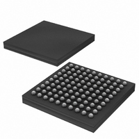
IC TXRX DS3/E3 100-CSBGA
Manufacturer
Maxim Integrated Products
Datasheet
1.DS3170.pdf
(230 pages)
Specifications of DS3170N+
Function
Single-Chip Transceiver
Interface
DS3, E3
Number Of Circuits
1
Voltage - Supply
3.135 V ~ 3.465 V
Current - Supply
120mA
Operating Temperature
-40°C ~ 85°C
Mounting Type
Surface Mount
Package / Case
100-LBGA
Includes
DS3 Framers, E3 Framers, HDLC Controller, On-Chip BERTs
Lead Free Status / RoHS Status
Lead free / RoHS Compliant
Power (watts)
-


4.5 Transmit DS3/E3 Formatter Features
4.6 Transmit DS3/E3 LIU Features
4.7 Clock Rate Adapter Features
4.8 HDLC Controller Features
4.9 FEAC Controller Features
Frame insertion for M23 and C-bit parity DS3, G.751 E3 and G.832 E3
B3ZS/HDB3 encoding
Formatter pass-through mode for clear channel applications and externally defined frame formats
Generation of RAI, AIS, DS3 idle signal, and G.832-E3 RDI
Automatic or manual insertion of bipolar violations (BPVs), excessive zeroes (EXZ) occurrences, F-bit errors,
M-bit errors, FAS errors, P-bit parity errors, CP-bit parity errors, BIP-8 errors, and far end block errors (FEBE)
The E3 national bit (Sn) can be sourced from a control register, from the HDLC controller, or from the FEAC
controller
Most framing overhead fields can be sourced from transmit overhead port
HDLC controller with 256 byte FIFO for DS3 path maintenance data link (PMDL), G.751 national bit, or G.832
NR or GC channels
FEAC controller for DS3 FEAC channel can be configured to send one codeword, one codeword continuously,
or two different codewords back-to-back to send DS3 Line Loopback commands
16-byte Trail Trace Buffer sources the G.832 trail access point identifier
Insertion of G.832 payload type, and timing marker bits from registers
DS3 M23 C-bits configurable as payload or overhead; as overhead they can be controlled from registers or the
transmit overhead port
Drives standards-compliant DS3 and E3 waveshapes onto 75Ω coaxial cable
Waveshape template compliance over all cable lengths without LBO adjustment
Tri-state line driver outputs support protection switching applications
Line driver monitor circuit and alarm output
Wide 50±20% transmit clock duty cycle
Line Build-Out (LBO) control
Output driver monitor
Generation of the internally needed DS3 (44.736 MHz) and E3 (34.368 MHz) clocks a from single input
reference clock
Input reference clock can be 77.76 MHz, 51.84 MHz, 44.736MHz, 34.368 MHz, or 19.44 MHz
Internally derived clock can be used as references for LIU and jitter attenuator
Derived clock can be transmitted off-chip for external system use through TCLKO pin
Standards-compliant jitter and wander requirements
Designed to handle multiple LAPD messages without Host intervention
256 byte receive and transmit FIFOs are large enough to handle the three DS3 PMDL messages (Path ID, Idle
Signal ID, and Test Signal ID) that are sent and received once per second
Handles all of the normal Layer 2 tasks including zero stuffing/destuffing, FCS generation/checking, abort
generation/checking, flag generation/detection, and byte alignment
Programmable high or low water marks for the transmit and receive FIFOs
Terminates the Path Maintenance Data Link in DS3 C-bit Parity mode or the G.751 Sn bit or the G.832 NR or
GC channels
Designed to handle multiple FEAC codewords without Host intervention
Receive FEAC automatically validates incoming codewords and stores them in a 4-codeword FIFO
Transmit FEAC can be configured to send one codeword, one codeword continuously, or two different
codewords back-to-back to send DS3 Line Loopback commands
Terminates the FEAC channel in DS3 C-Bit Parity mode or the Sn bit in E3 mode
14 of 230
DS3170 DS3/E3 Single-Chip Transceiver
Related parts for DS3170N+
Image
Part Number
Description
Manufacturer
Datasheet
Request
R

Part Number:
Description:
IC TXRX DS3/E3 100-CSBGA
Manufacturer:
Maxim Integrated Products
Datasheet:

Part Number:
Description:
Network Controller & Processor ICs DS3-E3 Single-Chip T ransceiver T3-E3 Fra
Manufacturer:
Maxim Integrated Products
Datasheet:
Part Number:
Description:
MAX7528KCWPMaxim Integrated Products [CMOS Dual 8-Bit Buffered Multiplying DACs]
Manufacturer:
Maxim Integrated Products
Datasheet:
Part Number:
Description:
Single +5V, fully integrated, 1.25Gbps laser diode driver.
Manufacturer:
Maxim Integrated Products
Datasheet:
Part Number:
Description:
Single +5V, fully integrated, 155Mbps laser diode driver.
Manufacturer:
Maxim Integrated Products
Datasheet:
Part Number:
Description:
VRD11/VRD10, K8 Rev F 2/3/4-Phase PWM Controllers with Integrated Dual MOSFET Drivers
Manufacturer:
Maxim Integrated Products
Datasheet:
Part Number:
Description:
Highly Integrated Level 2 SMBus Battery Chargers
Manufacturer:
Maxim Integrated Products
Datasheet:
Part Number:
Description:
Current Monitor and Accumulator with Integrated Sense Resistor; ; Temperature Range: -40°C to +85°C
Manufacturer:
Maxim Integrated Products
Part Number:
Description:
TSSOP 14/A°/RS-485 Transceivers with Integrated 100O/120O Termination Resis
Manufacturer:
Maxim Integrated Products
Part Number:
Description:
TSSOP 14/A°/RS-485 Transceivers with Integrated 100O/120O Termination Resis
Manufacturer:
Maxim Integrated Products
Part Number:
Description:
QFN 16/A°/AC-DC and DC-DC Peak-Current-Mode Converters with Integrated Step
Manufacturer:
Maxim Integrated Products
Part Number:
Description:
TDFN/A/65V, 1A, 600KHZ, SYNCHRONOUS STEP-DOWN REGULATOR WITH INTEGRATED SWI
Manufacturer:
Maxim Integrated Products
Part Number:
Description:
Integrated Temperature Controller f
Manufacturer:
Maxim Integrated Products
Part Number:
Description:
SOT23-6/I°/45MHz to 650MHz, Integrated IF VCOs with Differential Output
Manufacturer:
Maxim Integrated Products
Part Number:
Description:
SOT23-6/I°/45MHz to 650MHz, Integrated IF VCOs with Differential Output
Manufacturer:
Maxim Integrated Products