DS3170N+ Maxim Integrated Products, DS3170N+ Datasheet - Page 156
DS3170N+
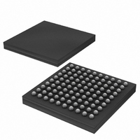
Manufacturer Part Number
DS3170N+
Description
IC TXRX DS3/E3 100-CSBGA
Manufacturer
Maxim Integrated Products
Datasheet
1.DS3170.pdf
(230 pages)
Specifications of DS3170N+
Function
Single-Chip Transceiver
Interface
DS3, E3
Number Of Circuits
1
Voltage - Supply
3.135 V ~ 3.465 V
Current - Supply
120mA
Operating Temperature
-40°C ~ 85°C
Mounting Type
Surface Mount
Package / Case
100-LBGA
Includes
DS3 Framers, E3 Framers, HDLC Controller, On-Chip BERTs
Lead Free Status / RoHS Status
Lead free / RoHS Compliant
Power (watts)
-


12.6 HDLC
12.6.1 HDLC Transmit Side Register Map
The transmit side utilizes five registers.
Table 12-16. Transmit Side HDLC Register Map
12.6.1.1 Register Bit Descriptions
Register Name:
Register Description:
Register Address:
Bit #
Name
Default
Bit #
Name
Default
Bits 12 to 8: Transmit HDLC Data Storage Available Level (TDAL[4:0]) – These five bits indicate the minimum
number of bytes ([TDAL*8}+1) that must be available for storage (do not contain data) in the Transmit FIFO for
HDLC data storage to be available. For example, a value of 21 (15h) results in HDLC data storage being available
(THDA=1) when the Transmit FIFO has 169 (A9h) bytes or more available for storage, and HDLC data storage not
being available (THDA=0) when the Transmit FIFO has 168 (A8h) bytes or less available for storage.
Bit 6: Transmit Packet Start Disable (TPSD) – When 0, the Transmit Packet Processor will continue sending
packets after the current packet end. When 1, the Transmit Packet Processor will stop sending packets after the
current packet end.
Bit 5: Transmit FCS Error Insertion (TFEI) – When 0, the calculated FCS (inverted CRC-16) is appended to the
packet. When 1, the inverse of the calculated FCS (noninverted CRC-16) is appended to the packet causing an
FCS error. This bit is ignored if transmit FCS processing is disabled (TFPD = 1).
Bit 4: Transmit Inter-frame Fill Value (TIFV) – When 0, inter-frame fill is done with the flag sequence (7Eh).
When 1, inter-frame fill is done with all ‘1’s.
Bit 3: Transmit Bit Reordering Enable (TBRE) – When 0, bit reordering is disabled (The first bit transmitted is the
LSB of the Transmit FIFO Data byte TFD[0]). When 1, bit reordering is enabled (The first bit transmitted is the MSB
of the Transmit FIFO Data byte TFD[7]).
Bit 2: Transmit Data Inversion Enable (TDIE) – When 0, the outgoing data is directly output from packet
processing. When 1, the outgoing data is inverted before being output from packet processing.
Address
0AAh
0ACh
0AEh
0A0h
0A2h
0A4h
0A6h
0A8h
15
HDLC.TCR
HDLC.TFDR
HDLC.TSR
HDLC.TSRL
HDLC.TSRIE
--
--
0
7
0
Register
--
--
--
TPSD
14
--
0
6
0
HDLC Transmit Control Register
HDLC Transmit FIFO Data Register
HDLC Transmit Status Register
HDLC Transmit Status Register Latched
HDLC Transmit Status Register Interrupt Enable
Unused
Unused
Unused
HDLC.TCR
HDLC Transmit Control Register
0A0h
Register Description
TFEI
13
--
0
5
0
156 of 230
TDAL4
TIFV
12
0
4
0
TDAL3
TBRE
11
1
3
0
DS3170 DS3/E3 Single-Chip Transceiver
TDAL2
TDIE
10
0
2
0
TDAL1
TFPD
9
0
1
0
TDAL0
TFRST
8
0
0
0
Related parts for DS3170N+
Image
Part Number
Description
Manufacturer
Datasheet
Request
R

Part Number:
Description:
IC TXRX DS3/E3 100-CSBGA
Manufacturer:
Maxim Integrated Products
Datasheet:

Part Number:
Description:
Network Controller & Processor ICs DS3-E3 Single-Chip T ransceiver T3-E3 Fra
Manufacturer:
Maxim Integrated Products
Datasheet:
Part Number:
Description:
MAX7528KCWPMaxim Integrated Products [CMOS Dual 8-Bit Buffered Multiplying DACs]
Manufacturer:
Maxim Integrated Products
Datasheet:
Part Number:
Description:
Single +5V, fully integrated, 1.25Gbps laser diode driver.
Manufacturer:
Maxim Integrated Products
Datasheet:
Part Number:
Description:
Single +5V, fully integrated, 155Mbps laser diode driver.
Manufacturer:
Maxim Integrated Products
Datasheet:
Part Number:
Description:
VRD11/VRD10, K8 Rev F 2/3/4-Phase PWM Controllers with Integrated Dual MOSFET Drivers
Manufacturer:
Maxim Integrated Products
Datasheet:
Part Number:
Description:
Highly Integrated Level 2 SMBus Battery Chargers
Manufacturer:
Maxim Integrated Products
Datasheet:
Part Number:
Description:
Current Monitor and Accumulator with Integrated Sense Resistor; ; Temperature Range: -40°C to +85°C
Manufacturer:
Maxim Integrated Products
Part Number:
Description:
TSSOP 14/A°/RS-485 Transceivers with Integrated 100O/120O Termination Resis
Manufacturer:
Maxim Integrated Products
Part Number:
Description:
TSSOP 14/A°/RS-485 Transceivers with Integrated 100O/120O Termination Resis
Manufacturer:
Maxim Integrated Products
Part Number:
Description:
QFN 16/A°/AC-DC and DC-DC Peak-Current-Mode Converters with Integrated Step
Manufacturer:
Maxim Integrated Products
Part Number:
Description:
TDFN/A/65V, 1A, 600KHZ, SYNCHRONOUS STEP-DOWN REGULATOR WITH INTEGRATED SWI
Manufacturer:
Maxim Integrated Products
Part Number:
Description:
Integrated Temperature Controller f
Manufacturer:
Maxim Integrated Products
Part Number:
Description:
SOT23-6/I°/45MHz to 650MHz, Integrated IF VCOs with Differential Output
Manufacturer:
Maxim Integrated Products
Part Number:
Description:
SOT23-6/I°/45MHz to 650MHz, Integrated IF VCOs with Differential Output
Manufacturer:
Maxim Integrated Products