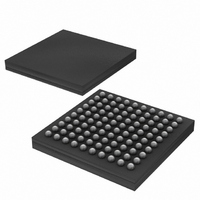
DS3170N+ Maxim Integrated Products, DS3170N+ Datasheet - Page 15

DS3170N+
Manufacturer Part Number
DS3170N+
Description
IC TXRX DS3/E3 100-CSBGA
Manufacturer
Maxim Integrated Products
Datasheet
1.DS3170.pdf
(230 pages)
Specifications of DS3170N+
Function
Single-Chip Transceiver
Interface
DS3, E3
Number Of Circuits
1
Voltage - Supply
3.135 V ~ 3.465 V
Current - Supply
120mA
Operating Temperature
-40°C ~ 85°C
Mounting Type
Surface Mount
Package / Case
100-LBGA
Includes
DS3 Framers, E3 Framers, HDLC Controller, On-Chip BERTs
Lead Free Status / RoHS Status
Lead free / RoHS Compliant
Power (watts)
-
- Current page: 15 of 230
- Download datasheet (3Mb)
4.10 Trail Trace Buffer Features
4.11 Bit Error-Rate Tester (BERT) Features
4.12 Loopback Features
4.13 Microprocessor Interface Features
4.14 Slave Serial Peripheral Interface (SPI) Features
4.15 Test Features
Extraction and storage of the incoming G.832 trail access point identifier in a 16-byte receive register
Insertion of the outgoing trail access point identifier from a 16-byte transmit register
Receive trace identifier unstable status indication
Generates and detects pseudo-random patterns and repetitive patterns from 1 to 32 bits in length
Supports pattern insertion/extraction in DS3/E3 payload, or entire data stream
Large 24-bit error counter allows testing to proceed for long periods without host intervention
Errors can be inserted in the generated BERT patterns for diagnostic purposes (single bit errors or specific bit-
error rates)
Off-line monitoring on the Receive BERT
LIU terminal loopback (transmit to receive) - ALB
Line facility loopback (receive to transmit) with optionally transmitting unframed all-one payload toward
system/trunk interface - LLB
Framer diagnostic loopback (transmit to receive) with optionally transmitting unframed all-one signal toward
line/tributary interface - DLB
Simultaneous line facility loopback (LLB) and framer diagnostic loopback (DLB)
Framer payload loopback (receive to transmit) with optionally transmitting unframed all-one payload toward
system/trunk interface - PLB
Multiplexed or nonmultiplexed 8- or 16-bit control port
Intel and Motorola bus compatible
Global reset input pin
Global interrupt output pin
Eight programmable I/O pins (GPIOx)
Three-wire synchronous serial data link operating in full duplex slave mode up to 10 Mbps
Glueless connection and fully compliant to Motorola popular communication processors such as MPC8260 and
microcontrollers such as M68HC11
Software provision ability for active phase of the serial clock (i.e. rising edge versus falling edge), bit ordering of
the serial data (most significant first versus least significant bit first)
Five pin JTAG port
All functional pins are inout pins in JTAG mode
Standard JTAG instructions: SAMPLE/PRELOAD, BYPASS, EXTEST, CLAMP, HIGHZ, IDCODE
Custom JTAG instructions to use RAM BIST
RAM BIST on all internal RAM
HIZ pin to force all digital output and inout pins into HIZ
TEST pin for manufacturing scan test modes
15 of 230
DS3170 DS3/E3 Single-Chip Transceiver
Related parts for DS3170N+
Image
Part Number
Description
Manufacturer
Datasheet
Request
R

Part Number:
Description:
IC TXRX DS3/E3 100-CSBGA
Manufacturer:
Maxim Integrated Products
Datasheet:

Part Number:
Description:
Network Controller & Processor ICs DS3-E3 Single-Chip T ransceiver T3-E3 Fra
Manufacturer:
Maxim Integrated Products
Datasheet:

Part Number:
Description:
MAX7528KCWPMaxim Integrated Products [CMOS Dual 8-Bit Buffered Multiplying DACs]
Manufacturer:
Maxim Integrated Products
Datasheet:

Part Number:
Description:
Single +5V, fully integrated, 1.25Gbps laser diode driver.
Manufacturer:
Maxim Integrated Products
Datasheet:

Part Number:
Description:
Single +5V, fully integrated, 155Mbps laser diode driver.
Manufacturer:
Maxim Integrated Products
Datasheet:

Part Number:
Description:
VRD11/VRD10, K8 Rev F 2/3/4-Phase PWM Controllers with Integrated Dual MOSFET Drivers
Manufacturer:
Maxim Integrated Products
Datasheet:

Part Number:
Description:
Highly Integrated Level 2 SMBus Battery Chargers
Manufacturer:
Maxim Integrated Products
Datasheet:

Part Number:
Description:
Current Monitor and Accumulator with Integrated Sense Resistor; ; Temperature Range: -40°C to +85°C
Manufacturer:
Maxim Integrated Products

Part Number:
Description:
TSSOP 14/A°/RS-485 Transceivers with Integrated 100O/120O Termination Resis
Manufacturer:
Maxim Integrated Products

Part Number:
Description:
TSSOP 14/A°/RS-485 Transceivers with Integrated 100O/120O Termination Resis
Manufacturer:
Maxim Integrated Products

Part Number:
Description:
QFN 16/A°/AC-DC and DC-DC Peak-Current-Mode Converters with Integrated Step
Manufacturer:
Maxim Integrated Products

Part Number:
Description:
TDFN/A/65V, 1A, 600KHZ, SYNCHRONOUS STEP-DOWN REGULATOR WITH INTEGRATED SWI
Manufacturer:
Maxim Integrated Products

Part Number:
Description:
Integrated Temperature Controller f
Manufacturer:
Maxim Integrated Products

Part Number:
Description:
SOT23-6/I°/45MHz to 650MHz, Integrated IF VCOs with Differential Output
Manufacturer:
Maxim Integrated Products

Part Number:
Description:
SOT23-6/I°/45MHz to 650MHz, Integrated IF VCOs with Differential Output
Manufacturer:
Maxim Integrated Products


