DS3170N+ Maxim Integrated Products, DS3170N+ Datasheet - Page 62
DS3170N+
Manufacturer Part Number
DS3170N+
Description
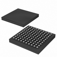
IC TXRX DS3/E3 100-CSBGA
Manufacturer
Maxim Integrated Products
Datasheet
1.DS3170.pdf
(230 pages)
Specifications of DS3170N+
Function
Single-Chip Transceiver
Interface
DS3, E3
Number Of Circuits
1
Voltage - Supply
3.135 V ~ 3.465 V
Current - Supply
120mA
Operating Temperature
-40°C ~ 85°C
Mounting Type
Surface Mount
Package / Case
100-LBGA
Includes
DS3 Framers, E3 Framers, HDLC Controller, On-Chip BERTs
Lead Free Status / RoHS Status
Lead free / RoHS Compliant
Power (watts)
-


Table 10-9. Receive Framer Pin Signal Timing Source Select
10.2.4 Clock Structures On Signal IO Pins
The signals on the input pins (TSOFI, TSER) can be used with any of the clock pins for setup/hold timing on clock
input and output pins. There will be a flop at each input whose clock is connected to the signal from the input or
output clock source pins with as little delay as possible from the signal on the clock IO pins. This means using the
input clock signal before the delays of the internal clock tree to clock the input signals, and using the output clock
signals used to drive the output clock pins to clock the input signals.
The signals on the output pins (TPOS/TDAT, TNEG, TSOFO/TDEN, RSER, RSOFO/RDEN) can be with any of the
clock sources for delay timing. There will be a flop at each output whose clock is connected to the signal from the
input or output clock source pins with as little delay as possible from the signal on the clock IO pins. This means
using the input clock signal before the delays of the internal clock tree to clock the input signals, and using the
output clock signals used to drive the output clock pins to clock the input signals.
1
1
1
0
0
0
0
0
0
0
0
0
PLB (011) or DLB (100) or ALB
DLB (100) or LLB & DLB (110)
DLB (100) or LLB & DLB (110)
not LLB, DLB or PLB (00X)
PLB (011) or DLB (100)
not LLB & DLB (110)
not LLB & DLB (110)
not DLB (100) and
not DLB (100) and
DLB&LLB (110)
LLB (010)
LBM[2:0]
(001)
XXX
XXX
XXX
X
X
X
X
X
X
0
1
0
1
0
1
62 of 230
X
X
X
X
X
X
X
X
X
X
0
1
0
1
1
0
0
0
0
0
1
1
1
1
RCLKO, TLCLK, TCLKO
RLCLK
No valid timing to any input clock pin
RCLKO, TLCLK, TCLKO
RCLKO, TLCLK, TCLKO
RCLKO, TCLKO
RCLKO, TLCLK
RCLKO
No valid timing to any input clock pin
TCLKI
RLCLK
No valid timing to any input clock pin
VALID TIMING TO THESE CLOCK PINS
DS3170 DS3/E3 Single-Chip Transceiver
Related parts for DS3170N+
Image
Part Number
Description
Manufacturer
Datasheet
Request
R

Part Number:
Description:
IC TXRX DS3/E3 100-CSBGA
Manufacturer:
Maxim Integrated Products
Datasheet:

Part Number:
Description:
Network Controller & Processor ICs DS3-E3 Single-Chip T ransceiver T3-E3 Fra
Manufacturer:
Maxim Integrated Products
Datasheet:
Part Number:
Description:
MAX7528KCWPMaxim Integrated Products [CMOS Dual 8-Bit Buffered Multiplying DACs]
Manufacturer:
Maxim Integrated Products
Datasheet:
Part Number:
Description:
Single +5V, fully integrated, 1.25Gbps laser diode driver.
Manufacturer:
Maxim Integrated Products
Datasheet:
Part Number:
Description:
Single +5V, fully integrated, 155Mbps laser diode driver.
Manufacturer:
Maxim Integrated Products
Datasheet:
Part Number:
Description:
VRD11/VRD10, K8 Rev F 2/3/4-Phase PWM Controllers with Integrated Dual MOSFET Drivers
Manufacturer:
Maxim Integrated Products
Datasheet:
Part Number:
Description:
Highly Integrated Level 2 SMBus Battery Chargers
Manufacturer:
Maxim Integrated Products
Datasheet:
Part Number:
Description:
Current Monitor and Accumulator with Integrated Sense Resistor; ; Temperature Range: -40°C to +85°C
Manufacturer:
Maxim Integrated Products
Part Number:
Description:
TSSOP 14/A°/RS-485 Transceivers with Integrated 100O/120O Termination Resis
Manufacturer:
Maxim Integrated Products
Part Number:
Description:
TSSOP 14/A°/RS-485 Transceivers with Integrated 100O/120O Termination Resis
Manufacturer:
Maxim Integrated Products
Part Number:
Description:
QFN 16/A°/AC-DC and DC-DC Peak-Current-Mode Converters with Integrated Step
Manufacturer:
Maxim Integrated Products
Part Number:
Description:
TDFN/A/65V, 1A, 600KHZ, SYNCHRONOUS STEP-DOWN REGULATOR WITH INTEGRATED SWI
Manufacturer:
Maxim Integrated Products
Part Number:
Description:
Integrated Temperature Controller f
Manufacturer:
Maxim Integrated Products
Part Number:
Description:
SOT23-6/I°/45MHz to 650MHz, Integrated IF VCOs with Differential Output
Manufacturer:
Maxim Integrated Products
Part Number:
Description:
SOT23-6/I°/45MHz to 650MHz, Integrated IF VCOs with Differential Output
Manufacturer:
Maxim Integrated Products