PMN25EN NXP Semiconductors, PMN25EN Datasheet
PMN25EN


Related parts for PMN25EN


PMN25EN Summary of contents
Page 1
... PMN25EN 30 V, 6.2 A N-channel Trench MOSFET Rev. 1 — 29 August 2011 1. Product profile 1.1 General description N-channel enhancement mode Field-Effect Transistor (FET small SOT457 (SC-74) small Surface-Mounted Device (SMD) plastic package using Trench MOSFET technology. 1.2 Features and benefits Logic level compatible Very fast switching 1.3 Applications ...
Page 2
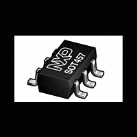
... Type number PMN25EN PMN25EN Product data sheet Description plastic surface-mounted package (TSOP6); 6 leads Marking code T8 All information provided in this document is subject to legal disclaimers. Rev. 1 — 29 August 2011 PMN25EN 30 V, 6.2 A N-channel Trench MOSFET Version SOT457 © NXP B.V. 2011. All rights reserved ...
Page 3
... °C amb ° °C amb 017aaa123 75 125 175 T (°C) j Fig 2. All information provided in this document is subject to legal disclaimers. Rev. 1 — 29 August 2011 PMN25EN 30 V, 6.2 A N-channel Trench MOSFET Min - -20 [ °C - [1] = 100 °C - ≤ 10 µ [ -55 -55 ...
Page 4
... Fig 3. Safe operating area; junction to ambient; continuous and peak drain currents as a function of drain-source voltage PMN25EN Product data sheet 1 2 All information provided in this document is subject to legal disclaimers. Rev. 1 — 29 August 2011 PMN25EN 30 V, 6.2 A N-channel Trench MOSFET 017aaa311 (1) (2) (3) (4) (5) (6) ...
Page 5
... Transient thermal impedance from junction to ambient as a function of pulse duration; typical values PMN25EN Product data sheet Conditions in free air – – All information provided in this document is subject to legal disclaimers. Rev. 1 — 29 August 2011 PMN25EN 30 V, 6.2 A N-channel Trench MOSFET Min Typ Max [1] - 200 230 [ ...
Page 6
... G(ext ° 1 ° All information provided in this document is subject to legal disclaimers. Rev. 1 — 29 August 2011 PMN25EN 30 V, 6.2 A N-channel Trench MOSFET Min Typ Max 1.5 2 100 - - 100 ...
Page 7
... PMN25EN Product data sheet 017aaa312 3.2 V 3.0 V 2.9 V 2 (V) DS Fig 7. All information provided in this document is subject to legal disclaimers. Rev. 1 — 29 August 2011 PMN25EN 30 V, 6.2 A N-channel Trench MOSFET – (A) –4 10 (1) (2) –5 10 – °C; V ...
Page 8
... 150 ° °C j Drain-source on-state resistance as a function of gate-source voltage; typical values 1.6 a 1.4 1.2 1.0 0.8 0.6 – function of junction temperature; typical values PMN25EN 017aaa315 (1) ( (V) GS 017aaa248 120 180 T (°C) j © NXP B.V. 2011. All rights reserved ...
Page 9
... Fig 13. Input, output and reverse transfer capacitances 017aaa313 7.5 10.0 Q (nC °C Fig 15. Gate charge waveform definitions All information provided in this document is subject to legal disclaimers. Rev. 1 — 29 August 2011 PMN25EN 30 V, 6.2 A N-channel Trench MOSFET – MHz (1) C ...
Page 10
... Fig 16. Source current as a function of source-drain voltage; typical values PMN25EN Product data sheet (A) 3 (1) ( 0.0 0.4 0.8 All information provided in this document is subject to legal disclaimers. Rev. 1 — 29 August 2011 PMN25EN 30 V, 6.2 A N-channel Trench MOSFET 017aaa318 1.2 V (V) DS © NXP B.V. 2011. All rights reserved ...
Page 11
... Test information Fig 17. Duty cycle definition PMN25EN Product data sheet duty cycle δ 006aaa812 All information provided in this document is subject to legal disclaimers. Rev. 1 — 29 August 2011 PMN25EN 30 V, 6.2 A N-channel Trench MOSFET © NXP B.V. 2011. All rights reserved ...
Page 12
... scale 3.1 1.7 3.0 0.6 0.95 2.7 1.3 2.5 0.2 REFERENCES JEDEC JEITA SC-74 All information provided in this document is subject to legal disclaimers. Rev. 1 — 29 August 2011 PMN25EN 30 V, 6.2 A N-channel Trench MOSFET detail 0.33 0.2 0.2 0.1 0.23 EUROPEAN PROJECTION SOT457 ...
Page 13
... Product data sheet 3.45 1.95 0.45 (6×) 0.7 (6×) 0.8 (6×) 2.4 5.3 1.45 (6×) 2.85 All information provided in this document is subject to legal disclaimers. Rev. 1 — 29 August 2011 PMN25EN 30 V, 6.2 A N-channel Trench MOSFET 0.55 solder lands (6×) solder resist solder paste occupied area Dimensions in mm sot457_fr 1.5 (4×) solder lands solder resist 0.45 (2×) ...
Page 14
... NXP Semiconductors 11. Revision history Table 8. Revision history Document ID Release date PMN25EN v.1 20110829 PMN25EN Product data sheet Data sheet status Change notice Product data sheet - All information provided in this document is subject to legal disclaimers. Rev. 1 — 29 August 2011 PMN25EN 30 V, 6.2 A N-channel Trench MOSFET ...
Page 15
... Characteristics sections of this document is not warranted. Constant or repeated exposure to limiting values will permanently and irreversibly affect the quality and reliability of the device. All information provided in this document is subject to legal disclaimers. Rev. 1 — 29 August 2011 PMN25EN 30 V, 6.2 A N-channel Trench MOSFET © NXP B.V. 2011. All rights reserved ...
Page 16
... TrenchMOS, TriMedia and UCODE — are trademarks of NXP B.V. HD Radio and HD Radio logo — are trademarks of iBiquity Digital Corporation. http://www.nxp.com salesaddresses@nxp.com All information provided in this document is subject to legal disclaimers. Rev. 1 — 29 August 2011 PMN25EN 30 V, 6.2 A N-channel Trench MOSFET © NXP B.V. 2011. All rights reserved ...
Page 17
... Please be aware that important notices concerning this document and the product(s) described herein, have been included in section ‘Legal information’. © NXP B.V. 2011. For more information, please visit: http://www.nxp.com For sales office addresses, please send an email to: salesaddresses@nxp.com PMN25EN All rights reserved. Date of release: 29 August 2011 Document identifier: PMN25EN ...