74LVC32245AEC,518 NXP Semiconductors, 74LVC32245AEC,518 Datasheet
74LVC32245AEC,518
Specifications of 74LVC32245AEC,518
74LVC32245AEC-T
935284953518
Available stocks


Related parts for 74LVC32245AEC,518


74LVC32245AEC,518 Summary of contents
Page 1
V tolerant; 3-state Rev. 01 — 20 August 2007 1. General description The 74LVC32245A is a 32-bit transceiver featuring non-inverting 3-state bus compatible outputs in both send and receive directions. The device ...
Page 2
... NXP Semiconductors 4. Functional diagram 1DIR A3 1A0 A5 1A1 A6 1A2 B5 1A3 B6 1A4 C5 1A5 C6 1A6 D5 1A7 D6 3DIR J3 3A0 J5 3A1 J6 3A2 K5 3A3 K6 3A4 L5 3A5 L6 3A6 M5 3A7 M6 Fig 1. Logic symbol 74LVC32245A_1 Product data sheet 32-bit bus transceiver with direction pin tolerant; 3-state 2DIR H3 1OE A4 2A0 E5 1B0 ...
Page 3
... NXP Semiconductors 5. Pinning information 5.1 Pinning 6 1A1 1A3 5 1A0 1A2 4 1OE GND 3 1DIR GND 2 1B0 1B2 1 1B1 1B3 A B Fig 2. Pin configuration 5.2 Pin description Table 2. Pin description Pin name nDIR ( nOE ( 1A[0:7] 1B[0:7] 2A[0:7] 2B[0:7] 3A[0:7] 3B[0:7] 4A[0:7] 4B[0:7] ...
Page 4
... NXP Semiconductors 7. Limiting values Table 4. Limiting values In accordance with the Absolute Maximum Rating System (IEC 60134). Voltages are referenced to GND (ground = 0 V). Symbol Parameter V supply voltage CC I input clamping current IK V input voltage I I output clamping current OK V output voltage O I output current ...
Page 5
... NXP Semiconductors 9. Static characteristics Table 6. Static characteristics At recommended operating conditions. Voltages are referenced to GND (ground = 0 V). Symbol Parameter +85 C amb V HIGH-level input voltage IH V LOW-level input voltage IL V HIGH-level output voltage OH V LOW-level output voltage OL I input leakage current I I OFF-state output current ...
Page 6
... NXP Semiconductors 10. Dynamic characteristics Table 7. Dynamic characteristics Voltages are referenced to GND (ground = 0 V). For test circuit see Symbol Parameter +85 C amb t propagation delay pd t enable time en t disable time dis t output skew time sk(o) C power dissipation PD capacitance [1] Typical values are measured at T ...
Page 7
... NXP Semiconductors nOE input output LOW-to-OFF OFF-to-LOW output HIGH-to-OFF OFF-to-HIGH < and V are typical output voltage levels that occur with the output load Fig 4. 3-state enable and disable times. 74LVC32245A_1 Product data sheet 32-bit bus transceiver with direction pin tolerant; 3-state ...
Page 8
... NXP Semiconductors Test data is given in Table 8. Definitions for test circuit Load resistance Load capacitance including jig and probe capacitance Termination resistance should be equal to output impedance External voltage for measuring switching times. EXT Fig 5. Load circuitry for switching times Table 8. Test data ...
Page 9
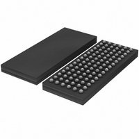
... NXP Semiconductors 12. Package outline LFBGA96: plastic low profile fine-pitch ball grid array package; 96 balls; body 13.5 x 5.5 x 1.05 mm ball A1 index area ball A1 index area DIMENSIONS (mm are the original dimensions) A UNIT max. 0.41 1.2 0.51 mm 1.5 0.31 0.9 0.41 OUTLINE VERSION IEC SOT536-1 Fig 6 ...
Page 10
... NXP Semiconductors 13. Abbreviations Table 9. Abbreviations Acronym Description DUT Device Under Test ESD ElectroStatic Discharge HBM Human Body Model MM Machine Model TTL Transistor-Transistor Logic 14. Revision history Table 10. Revision history Document ID Release date 74LVC32245A_1 20070820 74LVC32245A_1 Product data sheet 32-bit bus transceiver with direction pin tolerant; 3-state ...
Page 11
... For detailed and full information see the relevant full data sheet, which is available on request via the local NXP Semiconductors sales office. In case of any inconsistency or conflict with the short data sheet, the full data sheet shall prevail ...
Page 12
... NXP Semiconductors 17. Contents 1 General description . . . . . . . . . . . . . . . . . . . . . . 1 2 Features . . . . . . . . . . . . . . . . . . . . . . . . . . . . . . . 1 3 Ordering information . . . . . . . . . . . . . . . . . . . . . 1 4 Functional diagram . . . . . . . . . . . . . . . . . . . . . . 2 5 Pinning information . . . . . . . . . . . . . . . . . . . . . . 3 5.1 Pinning . . . . . . . . . . . . . . . . . . . . . . . . . . . . . . . 3 5.2 Pin description . . . . . . . . . . . . . . . . . . . . . . . . . 3 6 Functional description . . . . . . . . . . . . . . . . . . . 3 7 Limiting values Recommended operating conditions Static characteristics Dynamic characteristics . . . . . . . . . . . . . . . . . . 6 11 Waveforms . . . . . . . . . . . . . . . . . . . . . . . . . . . . . 6 12 Package outline . . . . . . . . . . . . . . . . . . . . . . . . . 9 13 Abbreviations . . . . . . . . . . . . . . . . . . . . . . . . . . 10 14 Revision history ...