GTLP16617MTDX Fairchild Semiconductor, GTLP16617MTDX Datasheet - Page 2
GTLP16617MTDX
Manufacturer Part Number
GTLP16617MTDX
Description
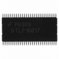
IC TRANSCVR 17BIT N-INV 56TSSOP
Manufacturer
Fairchild Semiconductor
Datasheet
1.GTLP16617MTDX.pdf
(9 pages)
Specifications of GTLP16617MTDX
Logic Type
Transceiver, Non-Inverting
Number Of Elements
1
Number Of Bits Per Element
17
Current - Output High, Low
32mA, 32mA
Voltage - Supply
3.15 V ~ 3.45 V
Operating Temperature
-40°C ~ 85°C
Mounting Type
Surface Mount
Package / Case
56-TSSOP
Lead Free Status / RoHS Status
Lead free / RoHS Compliant
Other names
GTLP16617MTDXTR
Available stocks
Company
Part Number
Manufacturer
Quantity
Price
Company:

Part Number:
GTLP16617MTDX
Manufacturer:
Fairchild Semiconductor
Quantity:
135


www.fairchildsemi.com
Pin Descriptions
Functional Description
The GTLP16617 is a 17 bit registered transceiver containing D-type flip-flop, latch and transparent modes of operation for
the data path and a GTLP translation of the CLKAB signal (CLKOUT). Data flow in each direction is controlled by the clock
enables (CEAB and CEBA), latch enables (LEAB and LEBA), clock (CLKAB and CLKBA) and output enables (OEAB and
OEBA). The clock enables (CEAB and CEBA) enable all 17 data bits. The output enables (OEAB and OEBA) control both
the 17 bits of data and the CLKOUT/CLKIN buffered clock paths and the OEAB is synchronous with the CLKAB signal. The
OEBA can not be synchronous since we are passing the clock through the device with data and we would need to generate
the CLKBA signal elsewhere. It should also be noted that the OEAB register is controlled by CLKAB only, and is also not
inhibited by the CEAB signal.
For A-to-B data flow, when CEAB is LOW, the device operates on the LOW-to-HIGH transition of CLKAB for the flip-flop
and on the HIGH-to-LOW transition of LEAB for the latch path. That is, if CEAB is LOW and LEAB is LOW the A data is
latched regardless as to the state of CLKAB (HIGH or LOW) and if LEAB is HIGH the device is in transparent mode. When
OEAB is registered LOW the outputs are active. When OEAB is registered HIGH the outputs are HIGH impedance. The
data flow of B-to-A is similar except that CEBA, OEBA, LEBA and CLKBA are used.
Truth Table
(Note 1)
Note 1: A-to-B data flow is shown. B-to-A data flow is similar but uses OEBA, LEBA, CLKBA, CEBA.
Note 2: LH edge on CLKAB is required when changing the input on OEAB pin.
Note 3: OEAB met set-up time prior to CLKAB LH transition
Note 4: Output level before the indicated steady state input conditions were established, provided CLKAB was HIGH prior to LEAB going LOW.
Note 5: Output level before the indicated steady state input conditions were established.
OEAB
OEBA
CEAB
CEBA
LEAB
LEBA
V
CLKAB
CLKBA
A1-A17
B1-B17
CLKIN
CLKOUT
REF
Pin Names
CEAB
X
X
X
H
L
L
L
L
A-to-B Clock
B-to-A Clock
GTLP Buffered Clock Output of CLKAB
A-to-B Output Enable (Active LOW)
B-to-A Output Enable (Active LOW)
A-to-B Clock Enable (Active LOW)
B-to-A Clock Enable (Active LOW)
A-to-B Latch Enable (Transparent HIGH)
B-to-A Latch Enable (Transparent HIGH)
GTLP Reference Voltage
A-to-B Data Inputs or B-to-A 3-STATE
Data Outputs
B-to-A Data Inputs or
A-to-B Open Drain Outputs
B-to-A Buffered Clock Output
OEAB (Note 2)
H
L
L
L
L
L
L
L
Description
Inputs
LEAB
X
H
H
L
L
L
L
L
CLKAB
H
X
X
X
L
2
Connection Diagram
A
H
H
X
X
X
L
L
X
B
B
Z (Note 3)
0
0
(Note 5)
Output
(Note 4)
(Note 5)
B
H
H
L
L
Latched storage
Clocked storage
Transparent
Clock inhibit
of A data
of A data
Mode
Related parts for GTLP16617MTDX
Image
Part Number
Description
Manufacturer
Datasheet
Request
R

Part Number:
Description:
Fairchild Semiconductor [IGBT MODULE]
Manufacturer:
Fairchild Semiconductor
Datasheet:

Part Number:
Description:
Discrete Semiconductor Modules
Manufacturer:
Fairchild Semiconductor
Part Number:
Description:
Discrete Semiconductor Modules
Manufacturer:
Fairchild Semiconductor
Part Number:
Description:
This N-Channel MOSFET is produced using Fairchild Semiconductor’s advanced Power Trench® process
Manufacturer:
Fairchild Semiconductor
Datasheet:
Part Number:
Description:
This N-Channel MOSFET is produced using Fairchild Semiconductor’s advanced Power Trench® process
Manufacturer:
Fairchild Semiconductor
Datasheet:
Part Number:
Description:
This N-Channel MOSFET is produced using Fairchild Semiconductor’s advanced PowerTrench® process
Manufacturer:
Fairchild Semiconductor
Datasheet:
Part Number:
Description:
This N-Channel MOSFET is produced using Fairchild Semiconductor’s advanced PowerTrench® process
Manufacturer:
Fairchild Semiconductor
Datasheet:
Part Number:
Description:
This N-Channel MOSFET is produced using Fairchild Semiconductor’s advanced Power Trench® process
Manufacturer:
Fairchild Semiconductor
Datasheet:
Part Number:
Description:
This N-Channel logic Level MOSFETs are produced using Fairchild Semiconductor‘s advanced Power Trench® process that has been special tailored to minimize the on-state resistance and yet maintain superior switching performance
Manufacturer:
Fairchild Semiconductor
Datasheet:
Part Number:
Description:
This N-Channel MOSFET is produced using Fairchild Semiconductor’s advanced Power Trench® process
Manufacturer:
Fairchild Semiconductor
Datasheet:
Part Number:
Description:
This N-Channel SyncFET™ is produced using Fairchild Semiconductor’s advanced PowerTrench® process
Manufacturer:
Fairchild Semiconductor
Datasheet:
Part Number:
Description:
This N-Channel SyncFET™ is produced using Fairchild Semiconductor’s advanced PowerTrench® process
Manufacturer:
Fairchild Semiconductor
Datasheet:
Part Number:
Description:
This N-Channel SyncFET™ is produced using Fairchild Semiconductor’s advanced PowerTrench® process
Manufacturer:
Fairchild Semiconductor
Datasheet:
Part Number:
Description:
This N-Channel logic Level MOSFETs are produced using Fairchild Semiconductor‘s advanced Power Trench® process that has been special tailored to minimize the on-state resistance and yet maintain superior switching performance
Manufacturer:
Fairchild Semiconductor
Datasheet:
Part Number:
Description:
This N-Channel MOSFET is produced using Fairchild Semiconductor’s advanced Power Trench® process that has been especially tailored to minimize the on-state resistance and yet maintain superior switching performance
Manufacturer:
Fairchild Semiconductor
Datasheet: