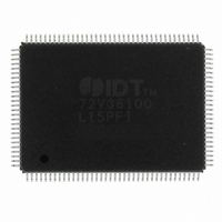
IDT72V36100L15PFI IDT, Integrated Device Technology Inc, IDT72V36100L15PFI Datasheet - Page 43

IDT72V36100L15PFI
Manufacturer Part Number
IDT72V36100L15PFI
Description
IC FIFO SYNC II 36BIT 128-TQFP
Manufacturer
IDT, Integrated Device Technology Inc
Series
72Vr
Datasheet
1.IDT72V36110L7-5BB.pdf
(48 pages)
Specifications of IDT72V36100L15PFI
Function
Synchronous
Memory Size
2.3K (64 x 36)
Data Rate
166MHz
Access Time
15ns
Voltage - Supply
3.15 V ~ 3.45 V
Operating Temperature
-40°C ~ 85°C
Mounting Type
Surface Mount
Package / Case
128-TQFP, 128-VQFP
Configuration
Dual
Density
2.25Mb
Access Time (max)
10ns
Word Size
36b
Organization
64Kx36
Sync/async
Synchronous
Expandable
Yes
Bus Direction
Uni-Directional
Package Type
TQFP
Clock Freq (max)
66.7MHz
Operating Supply Voltage (typ)
3.3V
Operating Supply Voltage (min)
3.15V
Operating Supply Voltage (max)
3.45V
Supply Current
40mA
Operating Temp Range
-40C to 85C
Operating Temperature Classification
Industrial
Mounting
Surface Mount
Pin Count
128
Lead Free Status / RoHS Status
Contains lead / RoHS non-compliant
Other names
72V36100L15PFI
800-1529
800-1529
Available stocks
Company
Part Number
Manufacturer
Quantity
Price
Company:
Part Number:
IDT72V36100L15PFI
Manufacturer:
IDT, Integrated Device Technology Inc
Quantity:
10 000
Company:
Part Number:
IDT72V36100L15PFI8
Manufacturer:
IDT, Integrated Device Technology Inc
Quantity:
10 000
SYSTEM INTERFACE PARAMETERS
TRST
NOTE:
1. During power up, TRST could be driven low or not be used since the JTAG circuit resets automatically. TRST is an optional JTAG reset.
NOTE:
1. 50pf loading on external output signals.
IDT72V36100/72V36110 3.3V HIGH DENSITY SUPERSYNC II
65,536 x 36 and 131,072 x 36
Data Output Hold
Data Output
TDI/
TMS
TDO
Parameter
TCK
Data Input
(1)
t
JTCKF
Symbol Test Conditions
t
t
DOH
t
DO
t
t
DS
DH
JRST
(1)
(1)
t
t
JTCKL
t
rise=3ns
fall=3ns
t
t
JTCKR
JRSR
t
t
TCK
DS
Min.
10
10
0
t
-
DH
IDT72V36100
IDT72V36110
Figure 31. Standard JTAG Timing
t
JTCKH
Max. Units
20
-
TM
-
-
36-BIT FIFO
ns
ns
ns
43
(V
NOTE:
1. Guaranteed by design.
JTAG AC ELECTRICAL
CHARACTERISTICS
JTAG Clock Input Period t
JTAG Clock HIGH
JTAG Clock Low
JTAG Clock Rise Time
JTAG Clock Fall Time
JTAG Reset
JTAG Reset Recovery
CC
= 3.3V
Parameter
±
5%; Tcase = 0°C to +85°C)
Symbol
t
t
t
t
t
t
TCK
JTCKH
JTCKL
JTCKR
JTCKF
JRST
JRSR
COMMERCIAL AND INDUSTRIAL
Conditions Min. Max. Units
Test
t
DO
-
-
-
-
-
-
-
TEMPERATURE RANGES
OCTOBER 22, 2008
100
40
40
50
50
-
-
TDO
5
5
-
-
-
-
-
(1)
(1)
6117 drw36
ns
ns
ns
ns
ns
ns
ns


