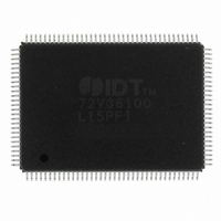
IDT72V36100L15PFI IDT, Integrated Device Technology Inc, IDT72V36100L15PFI Datasheet - Page 7

IDT72V36100L15PFI
Manufacturer Part Number
IDT72V36100L15PFI
Description
IC FIFO SYNC II 36BIT 128-TQFP
Manufacturer
IDT, Integrated Device Technology Inc
Series
72Vr
Datasheet
1.IDT72V36110L7-5BB.pdf
(48 pages)
Specifications of IDT72V36100L15PFI
Function
Synchronous
Memory Size
2.3K (64 x 36)
Data Rate
166MHz
Access Time
15ns
Voltage - Supply
3.15 V ~ 3.45 V
Operating Temperature
-40°C ~ 85°C
Mounting Type
Surface Mount
Package / Case
128-TQFP, 128-VQFP
Configuration
Dual
Density
2.25Mb
Access Time (max)
10ns
Word Size
36b
Organization
64Kx36
Sync/async
Synchronous
Expandable
Yes
Bus Direction
Uni-Directional
Package Type
TQFP
Clock Freq (max)
66.7MHz
Operating Supply Voltage (typ)
3.3V
Operating Supply Voltage (min)
3.15V
Operating Supply Voltage (max)
3.45V
Supply Current
40mA
Operating Temp Range
-40C to 85C
Operating Temperature Classification
Industrial
Mounting
Surface Mount
Pin Count
128
Lead Free Status / RoHS Status
Contains lead / RoHS non-compliant
Other names
72V36100L15PFI
800-1529
800-1529
Available stocks
Company
Part Number
Manufacturer
Quantity
Price
Company:
Part Number:
IDT72V36100L15PFI
Manufacturer:
IDT, Integrated Device Technology Inc
Quantity:
10 000
Company:
Part Number:
IDT72V36100L15PFI8
Manufacturer:
IDT, Integrated Device Technology Inc
Quantity:
10 000
NOTE:
1. Inputs should not change state after Master Reset.
PIN DESCRIPTION-CONTINUED (TQFP & PBGA PACKAGES)
NOTES:
1. Inputs should not change state after Master Reset.
2. These pins are for the JTAG port. Please refer to pages 43-47 and Figures 31-33.
PIN DESCRIPTION (PBGA PACKAGE ONLY)
IDT72V36100/72V36110 3.3V HIGH DENSITY SUPERSYNC II
65,536 x 36 and 131,072 x 36
SEN
WCLK/
WEN
V
WR
ASYR
ASYW
TCK
TDI
TDO
TMS
TRST
Symbol
Symbol
CC
(2)
(2)
(2)
(2)
(1)
(2)
(1)
Serial Enable
Write Clock/
Write Strobe
Write Enable
+3.3V Supply
Asynchronous
Read Port
Asynchronous
Write Port
JTAG Clock
JTAG Test Data
Input
JTAG Test Data
Output
JTAG Mode
JTAG Reset
Name
Name
I/O
I/O
O
I
I
I
I
I
I
I
I
I
I
SEN enables serial loading of programmable flag offsets.
If Synchronous operation of the write port has been selected, when enabled by WEN, the rising edge of WCLK
writes data into the FIFO. If Asynchronous operation of the write port has been selected, WR writes data into the FIFO
on a rising edge in an Asynchronous manner, (WEN should be tied to its active state). Asynchronous operation of
the WCLK/WR input is only available in the PBGA package.
WEN enables WCLK for writing data into the FIFO memory and offset registers.
These are V
One of four terminals required by IEEE Standard 1149.1-1990. During the JTAG boundary scan operation, test data
One of four terminals required by IEEE Standard 1149.1-1990. During the JTAG boundary scan operation, test data
A HIGH on this input during Master Reset will select Synchronous read operation for the output port. A LOW
will select Asynchronous operation. If Asynchronous is selected the FIFO must operate in IDT Standard mode.
A HIGH on this input during Master Reset will select Synchronous write operation for the input port. A LOW
will select Asynchronous operation.
Clock input for JTAG function. One of four terminals required by IEEE Standard 1149.1-1990. Test operations of the
device are synchronous to TCK. Data from TMS and TDI are sampled on the rising edge of TCK and outputs change
on the falling edge of TCK. If the JTAG function is not used this signal needs to be tied to GND.
serially loaded via the TDI on the rising edge of TCK to either the Instruction Register, ID Register and Bypass Register.
An internal pull-up resistor forces TDI HIGH if left unconnected.
serially loaded output via the TDO on the falling edge of TCK from either the Instruction Register, ID Register and Bypass
Register. This output is high impedance except when shifting, while in SHIFT-DR and SHIFT-IR controller states.
TMS is a serial input pin. One of four terminals required by IEEE Standard 1149.1-1990. TMS directs the device through
its TAP controller states. An internal pull-up resistor forces TMS HIGH if left unconnected.
TRST is an asynchronous reset pin for the JTAG controller. The JTAG TAP controller will automatically reset upon
power-up. If the JTAG function is not used then this signal should to be tied to GND.
CC
supply inputs and must be connected to the 3.3V supply rail.
TM
36-BIT FIFO
7
Description
Description
COMMERCIAL AND INDUSTRIAL
TEMPERATURE RANGES
OCTOBER 22, 2008


