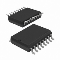
74HCT7403D,512 NXP Semiconductors, 74HCT7403D,512 Datasheet - Page 25

74HCT7403D,512
Manufacturer Part Number
74HCT7403D,512
Description
IC FIFO REGISTER 64X4 3ST 16SOIC
Manufacturer
NXP Semiconductors
Series
74HCTr
Datasheet
1.74HCT7403N112.pdf
(28 pages)
Specifications of 74HCT7403D,512
Function
Asynchronous, Synchronous
Memory Size
256 (64 x 4)
Data Rate
15MHz
Voltage - Supply
4.5 V ~ 5.5 V
Mounting Type
Surface Mount
Package / Case
16-SOIC (0.300", 7.5mm Width)
Logic Family
HCT
Logical Function
FIFO Register
Number Of Elements
1
Number Of Bits
4
Number Of Inputs
4
Number Of Outputs
4
High Level Output Current
-8mA
Low Level Output Current
8mA
Operating Supply Voltage (typ)
5V
Operating Supply Voltage (max)
5.5V
Operating Supply Voltage (min)
4.5V
Output Type
3-State
Polarity
Non-Inverting
Technology
CMOS
Mounting
Surface Mount
Pin Count
16
Operating Temp Range
-40C to 125C
Operating Temperature Classification
Automotive
Quiescent Current
50uA
Lead Free Status / RoHS Status
Lead free / RoHS Compliant
Operating Temperature
-
Access Time
-
Lead Free Status / Rohs Status
Compliant
Other names
74HCT7403D
74HCT7403D
933999390512
74HCT7403D
933999390512
Philips Semiconductors
Notes to Fig.21
1. FIFO
2. Load one word into FIFO
3. Data-out
4. DOR
5. DIR
6. DIR
7. DOR
September 1993
handbook, full pagewidth
4-Bit x 64-word FIFO register; 3-state
meeting data input set-up requirements of FIFO
output ready pulse, data is shifted into FIFO
anticipation of additional data
output stage.
B
B
A
A
B
and SO
and SO
goes HIGH; (ripple through delay after SI
and SI
and FIFO
A
/data-in
B
A
A
pulse HIGH; (ripple through delay after SI
go LOW; flag indicates input stage of FIFO
go HIGH automatically; the input stage of FIFO
B
initially empty, SO
B
Fig.21 FIFO to FIFO communication; input timing under empty condition.
transition; valid data arrives at FIFO
DOR B
DIR A
DOR A SI B
DIR B
Q nA
Q
SI A
nB
A
D
; SI pulse applied, results in DIR pulse
SO A
nB
1
A
V M
held HIGH in anticipation of data
(1)
V M
B
(1)
B
B
LOW) valid data is present one propagation delay later at the FIFO
ripple through
2
delay
25
A
A
LOW) data is unloaded from FIFO
B
output stage after a specified delay of the DOR flag,
3
is busy, shift-out of FIFO
V M
5
B
(1)
is again able to receive data, SO is held HIGH in
V M
4
(1)
ripple through
delay
6
7
A
V M
is complete
MGA666
(1)
74HC/HCT7403
A
as a result of the data
Product specification
B


