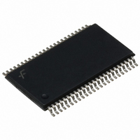
74VCX16374MTDX Fairchild Semiconductor, 74VCX16374MTDX Datasheet - Page 3

74VCX16374MTDX
Manufacturer Part Number
74VCX16374MTDX
Description
IC FLIP FLOP 16BIT D LV 48TSSOP
Manufacturer
Fairchild Semiconductor
Series
74VCXr
Type
D-Type Busr
Datasheet
1.74VCX16374MTDX.pdf
(10 pages)
Specifications of 74VCX16374MTDX
Function
Standard
Output Type
Tri-State Non Inverted
Number Of Elements
2
Number Of Bits Per Element
8
Frequency - Clock
250MHz
Delay Time - Propagation
1.5ns
Trigger Type
Positive Edge
Current - Output High, Low
24mA, 24mA
Voltage - Supply
1.2 V ~ 3.6 V
Operating Temperature
-40°C ~ 85°C
Mounting Type
Surface Mount
Package / Case
48-TSSOP
Logic Family
VCX
Technology
CMOS
Number Of Bits
16
Number Of Elements
2
Clock-edge Trigger Type
Positive-Edge
Polarity
Non-Inverting
Operating Supply Voltage (typ)
1.8/2.5/3.3V
Package Type
TSSOP
Propagation Delay Time
18.4ns
Low Level Output Current
24mA
High Level Output Current
-24mA
Frequency (max)
250MHz
Operating Supply Voltage (min)
1.2V
Operating Supply Voltage (max)
3.6V
Operating Temp Range
-40C to 85C
Operating Temperature Classification
Industrial
Mounting
Surface Mount
Pin Count
48
Lead Free Status / RoHS Status
Lead free / RoHS Compliant
Available stocks
Company
Part Number
Manufacturer
Quantity
Price
Company:
Part Number:
74VCX16374MTDX
Manufacturer:
AUK
Quantity:
2 107
Part Number:
74VCX16374MTDX
Manufacturer:
FAIRCHILD/仙童
Quantity:
20 000
Functional Description
The 74VCX16374 consists of sixteen edge-triggered
flip-flops with individual D-type inputs and 3-STATE true
outputs. The device is byte controlled with each byte func-
tioning identically, but independent of the other. The control
pins can be shorted together to obtain full 16-bit operation.
Each clock has a buffered clock and buffered Output
Enable common to all flip-flops within that byte. The
description which follows applies to each byte. Each
Logic Diagram
Please note that this diagram is provided only for the understanding of logic operations and should not be used to estimate propagation delays.
Byte 2 (8:15)
Byte 1 (0:7)
3
flip-flop will store the state of their individual I inputs that
meet the setup and hold time requirements on the
LOW-to-HIGH Clock (CP
Enable (OE
able at the outputs. When OE
the high impedance state. Operations of the OE
does not affect the state of the flip-flops.
n
) LOW, the contents of the flip-flops are avail-
n
) transition. With the Output
n
is HIGH, the outputs go to
www.fairchildsemi.com
n
input


