MM74HCT540WM Fairchild Semiconductor, MM74HCT540WM Datasheet

IC INVERTER 8-INPUT 20SOIC

MM74HCT540WM

Manufacturer Part Number
MM74HCT540WM
Description
IC INVERTER 8-INPUT 20SOIC
Manufacturer
Fairchild Semiconductor
Series
74HCTr
Datasheets

Specifications of MM74HCT540WM

Logic Type
Inverter
Number Of Inputs
8
Number Of Circuits
1
Current - Output High, Low
7.2mA, 7.2mA
Voltage - Supply
4.5 V ~ 5.5 V
Operating Temperature
-40°C ~ 85°C
Mounting Type
Surface Mount
Package / Case
20-SOIC (7.5mm Width)
Logic Device Type
Buffer / Line Driver, Inverting
Supply Voltage Range
4.5V To 5.5V
Logic Case Style
SOIC
No. Of Pins
20
Operating Temperature Range
-40°C To +85°C
Svhc
No SVHC (15-Dec-2010)
Rohs Compliant
Yes
Logic Family
HCT
Number Of Channels Per Chip
8
Polarity
Inverting
Supply Voltage (max)
5.5 V
Supply Voltage (min)
4.5 V
Maximum Operating Temperature
+ 85 C
Mounting Style
SMD/SMT
High Level Output Current
- 7.2 mA
Low Level Output Current
7.2 mA
Maximum Power Dissipation
500 mW
Minimum Operating Temperature
- 40 C
Number Of Lines (input / Output)
8 / 8
Output Type
3-State
Propagation Delay Time
30 ns at 5 V
Lead Free Status / RoHS Status
Lead free / RoHS Compliant

Available stocks

Company
Part Number
Manufacturer
Quantity
Price
Part Number:
MM74HCT540WM
Manufacturer:
Fairchild Semiconductor
Quantity:
1 782
© 2005 Fairchild Semiconductor Corporation
MM74HCT540WM
MM74HCT540SJ
MM74HCT540MTC
MM74HCT540N
MM74HCT541WM
MM74HCT541SJ
MM74HCT541MTC
MM74HCT541N
MM74HCT540 • MM74HCT541
Inverting Octal 3-STATE Buffer • Octal 3-STATE Buffer
General Description
The MM74HCT540 and MM74HCT541 3-STATE buffers
utilize advanced silicon-gate CMOS technology and are
general purpose high speed inverting and non-inverting
buffers. They possess high drive current outputs which
enable high speed operation even when driving large bus
capacitances. These circuits achieve speeds comparable
to low power Schottky devices, while retaining the low
power consumption of CMOS. Both devices are TTL input
compatible and have a fanout of 15 LS-TTL equivalent
inputs.
MM74HCT devices are intended to interface between TTL
and NMOS components and standard CMOS devices.
These parts are also plug-in replacements for LS-TTL
devices and can be used to reduce power consumption in
existing designs.
Ordering Code:
Devices also available in Tape and Reel. Specify by appending the suffix letter “X” to the ordering code.
Connection Diagrams
Pin Assignments for DIP, SOIC, SOP and TSSOP
Order Number
MM74HCT540
Top View
Package
Number
MTC20
MTC20
M20B
M20D
M20B
M20D
N20A
N20A
20-Lead Small Outline Integrated Circuit (SOIC), JEDEC MS-013, 0.300" Wide
20-Lead Small Outline Package (SOP), EIAJ TYPE II, 5.3mm Wide
20-Lead Thin Shrink Small Outline Package (TSSOP), JEDEC MO-153, 4.4mm Wide
20-Lead Plastic Dual-In-Line Package (PDIP), JEDEC MS-001, 0.300" Wide
20-Lead Small Outline Integrated Circuit (SOIC), JEDEC MS-013, 0.300" Wide
20-Lead Small Outline Package (SOP), EIAJ TYPE II, 5.3mm Wide
20-Lead Thin Shrink Small Outline Package (TSSOP), JEDEC MO-153, 4.4mm Wide
20-Lead Plastic Dual-In-Line Package (PDIP), JEDEC MS-001, 0.300" Wide
DS006040
The MM74HCT540 is an inverting buffer and the
MM74HCT541 is a non-inverting buffer. The 3-STATE con-
trol gate operates as a two-input NOR such that if either G1
or G2 are HIGH, all eight outputs are in the high-imped-
ance state.
In order to enhance PC board layout, the MM74HCT540
and MM74HCT541 offers a pinout having inputs and out-
puts on opposite sides of the package. All inputs are pro-
tected from damage due to static discharge by diodes to
V
Features
CC
TTL input compatible
Typical propagation delay: 12 ns
3-STATE outputs for connection to system buses
Low quiescent current: 80
Output current: 6 mA (min.)
and ground.
Package Description
MM74HCT541
Top View
P
A
February 1984
Revised May 2005
www.fairchildsemi.com

Related parts for MM74HCT540WM

MM74HCT540WM Summary of contents

Page 1

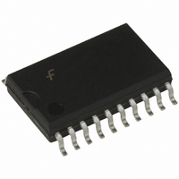
... These parts are also plug-in replacements for LS-TTL devices and can be used to reduce power consumption in existing designs. Ordering Code: Package Order Number Number MM74HCT540WM M20B 20-Lead Small Outline Integrated Circuit (SOIC), JEDEC MS-013, 0.300" Wide MM74HCT540SJ M20D 20-Lead Small Outline Package (SOP), EIAJ TYPE II, 5.3mm Wide MM74HCT540MTC MTC20 20-Lead Thin Shrink Small Outline Package (TSSOP), JEDEC MO-153, 4 ...

Page 2

Absolute Maximum Ratings (Note 2) Supply Voltage ( Input Voltage ( Output Voltage (V ) OUT Clamp Diode Current ( Output Current, per pin (I ) ...

Page 3

AC Electrical Characteristics MM74HCT540: V 5.0V ns Symbol Parameter Maximum Output PHL PLH Propagation Delay Maximum Output PZL PZH Enable Time Maximum Output ...

Page 4

AC Electrical Characteristics 5.0V ns, T MM74HCT541 Symbol Parameter Maximum Output PHL PLH Propagation Delay Maximum Output PZL PZH Enable Time Maximum Output ...

Page 5

Physical Dimensions inches (millimeters) unless otherwise noted 20-Lead Small Outline Integrated Circuit (SOIC), JEDEC MS-013, 0.300" Wide Package Number M20B 5 www.fairchildsemi.com ...

Page 6

Physical Dimensions inches (millimeters) unless otherwise noted (Continued) 20-Lead Small Outline Package (SOP), EIAJ TYPE II, 5.3mm Wide www.fairchildsemi.com Package Number M20D 6 ...

Page 7

Physical Dimensions inches (millimeters) unless otherwise noted (Continued) 20-Lead Thin Shrink Small Outline Package (TSSOP), JEDEC MO-153, 4.4mm Wide Package Number MTC20 7 www.fairchildsemi.com ...

Page 8

Physical Dimensions inches (millimeters) unless otherwise noted (Continued) 20-Lead Plastic Dual-In-Line Package (PDIP), JEDEC MS-001, 0.300" Wide Fairchild does not assume any responsibility for use of any circuitry described, no circuit patent licenses are implied and Fairchild reserves the right ...

Related keywords