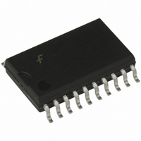
MM74HCT540WM Fairchild Semiconductor, MM74HCT540WM Datasheet - Page 2

MM74HCT540WM
Manufacturer Part Number
MM74HCT540WM
Description
IC INVERTER 8-INPUT 20SOIC
Manufacturer
Fairchild Semiconductor
Series
74HCTr
Specifications of MM74HCT540WM
Logic Type
Inverter
Number Of Inputs
8
Number Of Circuits
1
Current - Output High, Low
7.2mA, 7.2mA
Voltage - Supply
4.5 V ~ 5.5 V
Operating Temperature
-40°C ~ 85°C
Mounting Type
Surface Mount
Package / Case
20-SOIC (7.5mm Width)
Logic Device Type
Buffer / Line Driver, Inverting
Supply Voltage Range
4.5V To 5.5V
Logic Case Style
SOIC
No. Of Pins
20
Operating Temperature Range
-40°C To +85°C
Svhc
No SVHC (15-Dec-2010)
Rohs Compliant
Yes
Logic Family
HCT
Number Of Channels Per Chip
8
Polarity
Inverting
Supply Voltage (max)
5.5 V
Supply Voltage (min)
4.5 V
Maximum Operating Temperature
+ 85 C
Mounting Style
SMD/SMT
High Level Output Current
- 7.2 mA
Low Level Output Current
7.2 mA
Maximum Power Dissipation
500 mW
Minimum Operating Temperature
- 40 C
Number Of Lines (input / Output)
8 / 8
Output Type
3-State
Propagation Delay Time
30 ns at 5 V
Lead Free Status / RoHS Status
Lead free / RoHS Compliant
Available stocks
Company
Part Number
Manufacturer
Quantity
Price
Company:
Part Number:
MM74HCT540WM
Manufacturer:
Fairchild Semiconductor
Quantity:
1 782
www.fairchildsemi.com
V
V
V
V
I
I
I
IN
OZ
CC
Symbol
Absolute Maximum Ratings
(Note 2)
DC Electrical Characteristics
V
Note 4: Measured per input. All other inputs at V
IH
IL
OH
OL
CC
Supply Voltage (V
DC Input Voltage (V
DC Output Voltage (V
Clamp Diode Current (I
DC Output Current, per pin (I
DC V
Storage Temperature Range (T
Power Dissipation (P
Lead Temperature (T
(Note 3)
S.O. Package only
(Soldering 10 seconds)
5V
CC
Minimum HIGH Level
Input Voltage
Maximum LOW Level
Input Voltage
Minimum HIGH Level
Output Voltage
Maximum LOW Level
Voltage
Maximum Input
Current
Maximum 3-STATE
Output Leakage
Current
Maximum Quiescent
Supply Current
r
or GND Current, per pin (I
10% (unless otherwise specified)
Parameter
CC
IN
)
D
L
)
OUT
)
)
IK
, I
)
OK
OUT
)
STG
)
CC
V
|I
|I
|I
V
|I
|I
|I
V
V
G
V
I
V
)
OUT
OUT
OUT
OUT
OUT
OUT
OUT
IN
IN
IN
OUT
IN
IN
CC
)
V
|
|
|
|
|
|
or GND.
V
V
V
V
2.4V or 0.5V (Note 4)
IH
0
1.5 to V
0.5 to V
IH
IH
CC
CC
V
20
6.0 mA, V
7.2 mA, V
20
6.0 mA, V
7.2 mA, V
65
P
CC
Conditions
or V
or V
A
or GND
or GND
q
P
P
(Note 1)
0.5 to
C to
A
A
or GND
IL
IL
CC
CC
600 mW
500 mW
r
r
r
CC
CC
CC
CC
20 mA
35 mA
70 mA
150
260
7.0V
1.5V
0.5V
4.5V
5.5V
4.5V
5.5V
q
q
C
C
2
Recommended Operating
Conditions
Note 1: Absolute Maximum Ratings are those values beyond which dam-
age to the device may occur.
Note 2: Unless otherwise specified all voltages are referenced to ground.
Note 3: Power Dissipation temperature derating — plastic “N” package:
12 mW/
Supply Voltage (V
DC Input or Output Voltage
Operating Temperature Range (T
Input Rise or Fall Times
Typ
V
(V
(t
4.2
5.2
0.2
0.2
0.6
CC
0
r
, t
IN
T
q
A
f
C from 65
, V
)
25
OUT
V
q
CC
C
3.98
4.98
0.26
0.26
r
r
2.0
0.8
0.1
8.0
1.0
0.1
0.5
)
q
C to 85
0.1
CC
T
q
A
)
C.
Guaranteed Limits
V
CC
40 to 85
3.84
4.84
0.33
0.33
r
r
2.0
0.8
0.1
1.3
80
1.0
5.0
0.1
q
C T
A
)
A
Min
4.5
0
40
V
CC
55 to 125
r
r
160
2.0
0.8
3.7
4.7
0.1
0.4
0.4
1.5
1.0
10
0.1
Max
V
500
5.5
CC
85
q
C
Units
Units
q
ns
V
V
mA
C
P
P
P
V
V
V
V
V
V
V
V
A
A
A


