CD4019BCN Fairchild Semiconductor, CD4019BCN Datasheet

IC GATE AND/OR QUAD 16-DIP

CD4019BCN

Manufacturer Part Number
CD4019BCN
Description
IC GATE AND/OR QUAD 16-DIP
Manufacturer
Fairchild Semiconductor
Series
4000Br
Datasheet

Specifications of CD4019BCN

Logic Type
AND/OR Gate
Number Of Circuits
4
Number Of Inputs
2, 2
Schmitt Trigger Input
No
Output Type
Single-Ended
Current - Output High, Low
3mA, 10mA
Voltage - Supply
3 V ~ 15 V
Operating Temperature
-55°C ~ 125°C
Mounting Type
Through Hole
Package / Case
16-DIP (0.300", 7.62mm)
Lead Free Status / RoHS Status
Contains lead / RoHS non-compliant
Other names
4019
4019B
CD4019

Available stocks

Company
Part Number
Manufacturer
Quantity
Price
Part Number:
CD4019BCN
Quantity:
5 510
Part Number:
CD4019BCN
Manufacturer:
HAR
Quantity:
5 510
Part Number:
CD4019BCN
Manufacturer:
ST
0
Part Number:
CD4019BCN
Manufacturer:
FAIRCHILD/仙童
Quantity:
20 000
© 2002 Fairchild Semiconductor Corporation
CD4019BCM
CD4019BCN
CD4019BC
Quad AND-OR Select Gate
General Description
The CD4019BC is a complementary MOS quad AND-OR
select gate. Low power and high noise margin over a wide
voltage range is possible through implementation of N- and
P-channel enhancement mode transistors. These comple-
mentary MOS (CMOS) transistors provide the building
blocks for the 4 “AND-OR select” gate configurations, each
consisting of two 2-input AND gates driving a single 2-input
OR gate. Selection is accomplished by control bits K
K
age.
Ordering Code:
Devices also available in Tape and Reel. Specify by appending the suffix letter “X” to the ordering code.
Connection Diagram
Order Number
B
. All inputs are protected against static discharge dam-
Package Number
M16A
N16E
16-Lead Small Outline Integrated Circuit (SOIC), JEDEC MS-012, 0.150" Narrow
16-Lead Plastic Dual-In-Line Package (PDIP), JEDEC MS-001, 0.300" Wide
DS005952
A
and
Top View
Features
Applications
• AND-OR select gating
• Shift-right/shift-left registers
• True/complement selection
• AND/OR/EXCLUSIVE-OR selection
Wide supply voltage range:
High noise immunity: 0.45 V
Low power TTL compatibility: Fan out of 2 driving 74L
or 1 driving 74LS
Package Description
October 1987
Revised April 2002
DD
3.0V to 15V
(typ.)
www.fairchildsemi.com

Related parts for CD4019BCN

CD4019BCN Summary of contents

Page 1

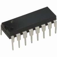
... Package Number CD4019BCM M16A 16-Lead Small Outline Integrated Circuit (SOIC), JEDEC MS-012, 0.150" Narrow CD4019BCN N16E 16-Lead Plastic Dual-In-Line Package (PDIP), JEDEC MS-001, 0.300" Wide Devices also available in Tape and Reel. Specify by appending the suffix letter “X” to the ordering code. ...

Page 2

Schematic Diagram Schematic diagram for identical stages www.fairchildsemi.com 2 ...

Page 3

Absolute Maximum Ratings (Note 2) Supply Voltage ( Input Voltage ( Storage Temperature Range ( Power Dissipation ( Dual-In-Line Small Outline Lead Temperature ( (Soldering, 10 seconds) ...

Page 4

AC Electrical Characteristics pF 200k, unless otherwise specified Symbol Parameter t , Propagation Delay, PHL t Input to Output PLH t HIGH-to-LOW Level THL Transition Time t LOW-to-HIGH Level TLH Transition ...

Page 5

Physical Dimensions inches (millimeters) unless otherwise noted 16-Lead Small Outline Integrated Circuit (SOIC), JEDEC MS-012, 0.150" Narrow Package Number M16A 5 www.fairchildsemi.com ...

Page 6

Physical Dimensions inches (millimeters) unless otherwise noted (Continued) 16-Lead Plastic Dual-In-Line Package (PDIP), JEDEC MS-001, 0.300" Wide Fairchild does not assume any responsibility for use of any circuitry described, no circuit patent licenses are implied and Fairchild reserves the right ...

Related keywords