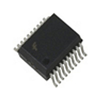
74LCX573SJX Fairchild Semiconductor, 74LCX573SJX Datasheet - Page 2

74LCX573SJX
Manufacturer Part Number
74LCX573SJX
Description
IC LATCH OCT LV 5V I/O 20SOP
Manufacturer
Fairchild Semiconductor
Series
74LCXr
Type
D-Typer
Datasheet
1.74LCX573MTC.pdf
(14 pages)
Specifications of 74LCX573SJX
Logic Type
D-Type Transparent Latch
Circuit
8:8
Output Type
Tri-State
Voltage - Supply
2 V ~ 3.6 V
Independent Circuits
1
Delay Time - Propagation
1.5ns
Current - Output High, Low
24mA, 24mA
Operating Temperature
-40°C ~ 85°C
Mounting Type
Surface Mount
Package / Case
20-SOIC (7.5mm Width)
Logic Family
LCX
Number Of Bits
8
Number Of Elements
1
Latch Mode
Transparent
Polarity
Non-Inverting
Technology
CMOS
Package Type
SOP
Propagation Delay Time
10.5ns
Operating Supply Voltage (typ)
2.5/3.3V
High Level Output Current
-24mA
Low Level Output Current
24mA
Operating Supply Voltage (min)
2V
Operating Supply Voltage (max)
3.6V
Operating Temp Range
-40C to 85C
Operating Temperature Classification
Industrial
Mounting
Surface Mount
Pin Count
20
Lead Free Status / RoHS Status
Lead free / RoHS Compliant
©2006 Fairchild Semiconductor Corporation
74LCX573 Rev. 1.6.0
Connection Diagrams
Pin Descriptions
Logic Diagram
Please note that this diagram is provided only for the understanding of logic operations and should not be used to estimate
propagation delays.
D
LE
OE
O
Pin Names
0
0
–D
–O
7
7
Pad Assignments for DQFN
OE
LE
SOIC, SOP, SSOP, TSSOP
GND
OE
D
D
D
D
D
D
D
D
Pin Assignments for
Data Inputs
Latch Enable Input
3-STATE Output Enable Input
3-STATE Latch Outputs
0
1
2
3
4
5
6
7
D
D
D
D
D
D
D
D
D
0
1
2
3
4
5
6
7
0
1
2
3
4
5
6
7
8
9
10
(Top View)
D
2
3
4
5
6
7
8
9
GND
LE
OE
10
1
Q
O
D
0
V
Description
LE
11
20
1
CC
20
19
18
17
16
15
14
13
12
11
D
19
18
17
16
15
14
13
12
LE
O
O
O
O
O
O
O
O
Q
V
O
O
O
O
O
O
O
O
LE
0
1
2
3
4
5
6
7
CC
0
1
2
3
4
5
6
7
D
O
2
1
D
LE
Q
D
O
3
2
D
LE
Q
D
O
2
4
3
D
Logic Symbol
Truth Table
H = HIGH Voltage
L = LOW Voltage
Z = High Impedance
X = Immaterial
O
Latch Enable
Functional Description
The LCX573 contains eight D-type latches with 3-STATE
output buffers. When the Latch Enable (LE) input is
HIGH, data on the D
condition the latches are transparent, i.e., a latch output
will change state each time its D input changes. When
LE is LOW the latches store the information that was
present on the D inputs a setup time preceding the
HIGH-to-LOW transition of LE. The 3-STATE buffers are
controlled by the Output Enable (OE) input. When OE is
LOW, the buffers are enabled. When OE is HIGH the
buffers are in the high impedance mode but this does not
interfere with entering new data into the latches.
0
LE
= Previous O
Q
OE
H
L
L
L
D
O
5
4
D
LE
Q
Inputs
D
O
0
6
5
OE
LE
LE
before HIGH-to-LOW transition of
H
H
X
D
L
D
O
0
0
LE
n
O
D
Q
1
1
inputs enters the latches. In this
O
D
D
O
2
2
7
6
D
O
D
3
3
D
O
LE
D
H
X
X
4
L
4
Q
D
O
5
5
O
O
D
7
6
6
O
D
7
7
Outputs
www.fairchildsemi.com
O
O
H
Z
L
n
0


