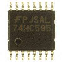
MM74HC595MTCX Fairchild Semiconductor, MM74HC595MTCX Datasheet - Page 8

MM74HC595MTCX
Manufacturer Part Number
MM74HC595MTCX
Description
IC SHIFT REGISTER 8-BIT 16-TSSOP
Manufacturer
Fairchild Semiconductor
Series
74HCr
Type
Not Requiredr
Datasheet
1.MM74HC595M.pdf
(14 pages)
Specifications of MM74HC595MTCX
Logic Type
Shift Register
Output Type
Standard
Number Of Elements
1
Number Of Bits Per Element
8
Function
Serial to Parallel
Voltage - Supply
2 V ~ 6 V
Operating Temperature
-40°C ~ 85°C
Mounting Type
Surface Mount
Package / Case
16-TSSOP
Counting Sequence
Serial to Serial/Parallel
Number Of Circuits
1
Logic Family
74HC
Propagation Delay Time
294 ns, 58 ns, 50 ns
Supply Voltage (max)
6 V
Maximum Operating Temperature
+ 85 C
Minimum Operating Temperature
- 40 C
Mounting Style
SMD/SMT
Operating Supply Voltage
2 V to 6 V
Technology
CMOS
Number Of Elements
1
Number Of Bits
8
Logical Function
Shift Register
Operating Supply Voltage (typ)
2.5/3.3/5V
Package Type
TSSOP
Operating Temp Range
-40C to 85C
Operating Supply Voltage (min)
2V
Operating Supply Voltage (max)
6V
Operating Temperature Classification
Industrial
Mounting
Surface Mount
Pin Count
16
Lead Free Status / RoHS Status
Lead free / RoHS Compliant
Other names
MM74HC595MTCX
MM74HC595MTCXTR
MM74HC595MTCXTR
Available stocks
Company
Part Number
Manufacturer
Quantity
Price
Company:
Part Number:
MM74HC595MTCX
Manufacturer:
FSC
Quantity:
100 000
Company:
Part Number:
MM74HC595MTCX
Manufacturer:
FSC
Quantity:
11 000
Part Number:
MM74HC595MTCX
Manufacturer:
FAIRCHILD/仙童
Quantity:
20 000
© 1983 Fairchild Semiconductor Corporation
MM74HC595 • Rev. 1.0.2
Electrical Characteristics
V
Note:
5.
Symbol
t
CC
THL
C
t
C
C
R
t
t
t
t
t
OUT
= 2.0−6.0V, C
W
S
R
S
H
,t
,t
PD
C
current consumption, I
IN
F
TLH
PD
determines the no load dynamic power consumption, P
Minimum Setup Time from
SER to SCK
Minimum Removal Time
from SCLR to SCK
Minimum Setup Time from
SCK to RCK
Minimum Hold Time from
SER to SCK
Minimum Pulse Width of
SCK or SCLR
Maximum Input Rise and
Fall Time, Clock
Maximum Output Rise and
Fall Time Q
Maximum Output Rise and
Fall Time Q’
Power Dissipation
Capacitance, Outputs
Enabled
Maximum Input Capacitance
Maximum Output
Capacitance
L
Parameter
(5)
= 50pF, t
A
H
-Q
H
S
= C
r
= t
PD
f
=6ns unless otherwise specified.
V
CC
f + I
R
G=V
G=GND
CC
L
=1kΩ, C
.
Conditions
CC
L
=50pF
8
2.0V
4.5V
6.0V
2.0V
4.5V
6.0V
2.0V
4.5V
6.0V
2.0V
4.5V
6.0V
2.0V
4.5V
6.0V
2.0V
4.5V
6.0V
2.0V
4.5V
6.0V
2.0V
4.5V
6.0V
V
D
CC
= C
PD
Typ.
150
V
90
15
30
25
T
9
8
7
6
5
CC
A
=25°C
2
f + I
1000
100
100
500
400
CC
20
17
50
10
20
17
80
16
14
60
12
10
75
15
13
10
20
9
5
5
5
Guaranteed Limits
V
CC
T
, and the no load dynamic
A
85°C
=-40 to
1000
125
125
100
500
400
25
21
63
13
11
25
21
20
18
75
15
13
95
19
16
10
20
5
5
5
to 125°C
T
1000
A
150
150
120
500
400
110
=-55
30
25
75
15
13
30
26
24
22
90
18
15
22
19
10
20
5
5
5
www.fairchildsemi.com
Units
pF
pF
pF
ns
ns
ns
ns
ns
ns
ns
ns


