74LCX257SJ Fairchild Semiconductor, 74LCX257SJ Datasheet

MULTIPLEXER QUAD 2IN LV 16SOP

74LCX257SJ

Manufacturer Part Number
74LCX257SJ
Description
MULTIPLEXER QUAD 2IN LV 16SOP
Manufacturer
Fairchild Semiconductor
Series
74LCXr
Type
Multiplexerr
Datasheet

Specifications of 74LCX257SJ

Circuit
4 x 2:1
Independent Circuits
1
Current - Output High, Low
24mA, 24mA
Voltage Supply Source
Single Supply
Voltage - Supply
2 V ~ 3.6 V
Operating Temperature
-40°C ~ 85°C
Mounting Type
Surface Mount
Package / Case
16-SOIC (5.3mm Width), 16-SO, 16-SOEIIJ
Logical Function
Mux
Configuration
4 x 2:1
Number Of Inputs
8
Number Of Outputs
4
Operating Supply Voltage (typ)
2.5/3.3V
Operating Supply Voltage (min)
2V
Operating Supply Voltage (max)
3.6V
Operating Temp Range
-40C to 85C
Operating Temperature Classification
Industrial
Mounting
Surface Mount
Pin Count
16
Package Type
SOEIAJ
Lead Free Status / RoHS Status
Lead free / RoHS Compliant
© 2000 Fairchild Semiconductor Corporation
74LCX257M
74LCX257SJ
74LCX257MTC
74LCX257
Low Voltage Quad 2-Input Multiplexer
with 5V Tolerant Inputs and Outputs
General Description
The LCX257 is a quad 2-input multiplexer with 3-STATE
outputs. Four bits of data from two sources can be selected
using a Common Data Select input. The four outputs
present the selected data in true (non inverted) form. The
outputs may be switched to a high impedance state by
placing a logic HIGH on the common Output Enable (OE)
input, allowing the outputs to interface directly with bus-ori-
ented systems.
The 74LCX257 is fabricated with advanced CMOS technol-
ogy to achieve high speed operation while maintaining
CMOS low power dissipation.
Ordering Code:
Devices also available in Tape and Reel. Specify by appending the suffix letter “X” to the ordering code.
Logic Symbols
Order Number
Package Number
MTC16
IEEE/IEC
M16A
M16D
16-Lead Small Outline Integrated Circuit (SOIC), JEDEC MS-012, 0.150 Narrow
16-Lead Small Outline Package (SOP), EIAJ TYPE II, 5.3mm Wide
16-Lead Thin Shrink Small Outline Package (TSSOP), JEDEC MO-153, 4.4mm Wide
DS012466
Features
Note 1: To ensure the high-impedance state during power up or down, OE
should be tied to V
resistor is determined by the current-sourcing capability of the driver.
Connection Diagram
Pin Descriptions
5V tolerant inputs and outputs
2.3V–3.6V V
6.0 ns t
Power down high impedance inputs and outputs
Supports live insertion/withdrawal (Note 1)
Implements patented noise/EMI reduction circuitry
Latch-up performance exceeds 500 mA
ESD performance:
S
OE
I
I
Z
Human body model
Machine model
Pin Names
0a
1a
a
–Z
Package Description
–I
–I
0d
1d
d
PD
max (V
CC
CC
through a pull-up resistor: the minimum value or the
specifications provided
Common Data Select Input
3-STATE Output Enable Input
Data Inputs from Source 0
Data Inputs from Source 1
3-STATE Multiplexer Outputs
CC
200V
3.3V, I
2000V
May 1995
Revised September 2000
n
Description
Z
n
), 10 A I
www.fairchildsemi.com
CC
max

Related parts for 74LCX257SJ

74LCX257SJ Summary of contents

Page 1

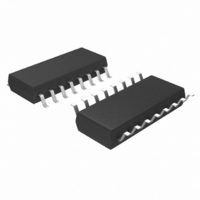
... Ordering Code: Order Number Package Number 74LCX257M M16A 16-Lead Small Outline Integrated Circuit (SOIC), JEDEC MS-012, 0.150 Narrow 74LCX257SJ M16D 16-Lead Small Outline Package (SOP), EIAJ TYPE II, 5.3mm Wide 74LCX257MTC MTC16 16-Lead Thin Shrink Small Outline Package (TSSOP), JEDEC MO-153, 4.4mm Wide Devices also available in Tape and Reel. Specify by appending the suffix letter “ ...

Page 2

Functional Description The LCX257 is a quad 2-input multiplexer with 3-STATE outputs. It selects four bits of data from two sources under control of a Common Data Select input. When the Select input is LOW, the I inputs are selected ...

Page 3

Absolute Maximum Ratings Symbol Parameter V Supply Voltage Input Voltage Output Voltage Input Diode Current Output Diode Current Output Source/Sink Current Supply ...

Page 4

DC Electrical Characteristics Symbol Parameter I Quiescent Supply Current CC I Increase in I per Input CC CC Note 5: Outputs disabled or 3-STATE only. AC Electrical Characteristics Symbol Parameter t Propagation Delay PHL PLH n t ...

Page 5

AC LOADING and WAVEFORMS FIGURE 1. AC Test Circuit (C Test t PLH t PZL t PZH Waveform for Inverting and Non-Inverting Functions Propagation Delay. Pulse Width and t rec 3-STATE Output Low Enable and Disable Times for Logic (Input ...

Page 6

Schematic Diagram Generic for LCX Family www.fairchildsemi.com 6 ...

Page 7

Physical Dimensions inches (millimeters) unless otherwise noted 16-Lead Small Outline Integrated Circuit (SOIC), JEDEC MS-012, 0.150 Narrow Package Number M16A 7 www.fairchildsemi.com ...

Page 8

Physical Dimensions inches (millimeters) unless otherwise noted (Continued) 16-Lead Small Outline Package (SOP), EIAJ TYPE II, 5.3mm Wide www.fairchildsemi.com Package Number M16D 8 ...

Page 9

Physical Dimensions inches (millimeters) unless otherwise noted (Continued) 16-Lead Thin Shrink Small Outline Package (TSSOP), JEDEC MO-153, 4.4mm Wide Fairchild does not assume any responsibility for use of any circuitry described, no circuit patent licenses are implied and Fairchild reserves ...

Related keywords