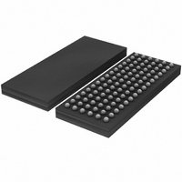
SSTUH32866EC/G,551 NXP Semiconductors, SSTUH32866EC/G,551 Datasheet - Page 7

SSTUH32866EC/G,551
Manufacturer Part Number
SSTUH32866EC/G,551
Description
IC BUFFER 1.8V 25BIT SOT536-1
Manufacturer
NXP Semiconductors
Datasheet
1.SSTUH32866ECG518.pdf
(28 pages)
Specifications of SSTUH32866EC/G,551
Logic Type
1:1, 1:2 Configurable Registered Buffer with Parity
Supply Voltage
1.7 V ~ 1.9 V
Number Of Bits
25, 14
Operating Temperature
0°C ~ 70°C
Mounting Type
Surface Mount
Package / Case
96-LFBGA
Lead Free Status / RoHS Status
Lead free / RoHS Compliant
Other names
935277966551
SSTUH32866EC/G-S
SSTUH32866EC/G-S
SSTUH32866EC/G-S
SSTUH32866EC/G-S
Philips Semiconductors
9397 750 14199
Product data sheet
6.2 Pin description
Table 2:
Symbol
GND
V
VREF
CK
CK
C0
C1
RESET
CSR
DCS
D1 to D25
DODT
DCKE
PAR_IN
Q1 to Q25,
Q2A to Q14A,
Q1B to Q14B
PPO
QCS, QCSA,
QCSB
QODT, QODTA,
QODTB
QCKE, QCKEA,
QCKEB
DD
Pin description
Pin
B3, B4, D3, D4,
F3, F4, H3, H4,
K3, K4, M3, M4,
P3, P4
A4, C3, C4, E3,
E4, G3, G4, J3,
J4, L3, L4, N3,
N4, R3, R4, T4
A3, T3
H1
J1
G6
G5
G2
J2
H2
G1
A2
[1]
[1]
[1]
[1]
[1]
[1]
[1]
1.8 V high-drive DDR2 configurable registered buffer with parity
Rev. 01 — 13 May 2005
Type
ground input
1.8 V nominal
0.9 V nominal
Differential input
Differential input
LVCMOS inputs
LVCMOS input
SSTL_18 input
SSTL_18 input
SSTL_18 input
SSTL_18 input
SSTL_18 input
1.8 V CMOS
outputs
1.8 V CMOS
output
1.8 V CMOS
output
1.8 V CMOS
output
1.8 V CMOS
output
Description
ground
power supply voltage
input reference voltage
positive master clock input
negative master clock input
Configuration control inputs; Register A
or Register B and 1 : 1 mode or 1 : 2
mode select.
Asynchronous reset input (active LOW).
Resets registers and disables VREF data
and clock.
Chip select inputs (active LOW). Disables
D1 to D25
inputs are HIGH.
Data input. Clocked in on the crossing of
the rising edge of CK and the falling edge
of CK.
The outputs of this register bit will not be
suspended by the DCS and CSR control.
The outputs of this register bit will not be
suspended by the DCS and CSR control.
Parity input. Arrives one clock cycle after
the corresponding data input.
Data outputs that are suspended by the
DCS and CSR control
Partial parity out. Indicates odd parity of
inputs D1 to D25
Data output that will not be suspended by
the DCS and CSR control.
Data output that will not be suspended by
the DCS and CSR control.
Data output that will not be suspended by
the DCS and CSR control.
© Koninklijke Philips Electronics N.V. 2005. All rights reserved.
[2]
SSTUH32866
outputs switching when both
[2]
.
[3]
.
7 of 28


