SSTUH32866EC/G,551 NXP Semiconductors, SSTUH32866EC/G,551 Datasheet - Page 9
SSTUH32866EC/G,551
Manufacturer Part Number
SSTUH32866EC/G,551
Description
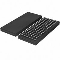
IC BUFFER 1.8V 25BIT SOT536-1
Manufacturer
NXP Semiconductors
Datasheet
1.SSTUH32866ECG518.pdf
(28 pages)
Specifications of SSTUH32866EC/G,551
Logic Type
1:1, 1:2 Configurable Registered Buffer with Parity
Supply Voltage
1.7 V ~ 1.9 V
Number Of Bits
25, 14
Operating Temperature
0°C ~ 70°C
Mounting Type
Surface Mount
Package / Case
96-LFBGA
Lead Free Status / RoHS Status
Lead free / RoHS Compliant
Other names
935277966551
SSTUH32866EC/G-S
SSTUH32866EC/G-S
SSTUH32866EC/G-S
SSTUH32866EC/G-S


Philips Semiconductors
9397 750 14199
Product data sheet
cascaded to the PAR_IN of the second register. The QERR output of the first register is
left floating and the valid error information is latched on the QERR output of the second
register.
If an error occurs and the QERR output is driven LOW, it stays latched LOW for two clock
cycles or until RESET is driven LOW. The DIMM-dependent signals (DCKE, DCS, DODT,
and CSR) are not included in the parity check computation.
The device supports low-power standby operation. When RESET is LOW, the differential
input receivers are disabled, and undriven (floating) data, clock and reference voltage
(VREF) inputs are allowed. In addition, when RESET is LOW all registers are reset, and
all outputs are forced LOW. The LVCMOS RESET input must always be held at a valid
logic HIGH or LOW level.
The device also supports low-power active operation by monitoring both system chip
select (DCS and CSR) inputs and will gate the Qn and PPO outputs from changing states
when both DCS and CSR inputs are HIGH. If either DCS or CSR input is LOW, the Qn
and PPO outputs will function normally. The RESET input has priority over the DCS and
CSR control and when driven LOW will force the Qn and PPO outputs LOW, and the
QERR output HIGH. If the DCS control functionality is not desired, then the CSR input can
be hard-wired to ground, in which case, the setup time requirement for DCS would be the
same as for the other Dn data inputs. To control the low-power mode with DCS only, then
the CSR input should be pulled up to V
To ensure defined outputs from the register before a stable clock has been supplied,
RESET must be held in the LOW state during power-up.
In the DDR2 RDIMM application, RESET is specified to be completely asynchronous with
respect to CK and CK. Therefore, no timing relationship can be guaranteed between the
two. When entering reset, the register will be cleared and the Qn outputs will be driven
LOW quickly, relative to the time to disable the differential input receivers. However, when
coming out of reset, the register will become active quickly, relative to the time to enable
the differential input receivers. As long as the data inputs are LOW, and the clock is stable
during the time from the LOW-to-HIGH transition of RESET until the input receivers are
fully enabled, the design of the SSTUH32866 must ensure that the outputs will remain
LOW, thus ensuring no glitches on the output.
1.8 V high-drive DDR2 configurable registered buffer with parity
Rev. 01 — 13 May 2005
DD
through a pull-up resistor.
© Koninklijke Philips Electronics N.V. 2005. All rights reserved.
SSTUH32866
9 of 28
Related parts for SSTUH32866EC/G,551
Image
Part Number
Description
Manufacturer
Datasheet
Request
R

Part Number:
Description:
NXP Semiconductors designed the LPC2420/2460 microcontroller around a 16-bit/32-bitARM7TDMI-S CPU core with real-time debug interfaces that include both JTAG andembedded trace
Manufacturer:
NXP Semiconductors
Datasheet:

Part Number:
Description:
NXP Semiconductors designed the LPC2458 microcontroller around a 16-bit/32-bitARM7TDMI-S CPU core with real-time debug interfaces that include both JTAG andembedded trace
Manufacturer:
NXP Semiconductors
Datasheet:
Part Number:
Description:
NXP Semiconductors designed the LPC2468 microcontroller around a 16-bit/32-bitARM7TDMI-S CPU core with real-time debug interfaces that include both JTAG andembedded trace
Manufacturer:
NXP Semiconductors
Datasheet:
Part Number:
Description:
NXP Semiconductors designed the LPC2470 microcontroller, powered by theARM7TDMI-S core, to be a highly integrated microcontroller for a wide range ofapplications that require advanced communications and high quality graphic displays
Manufacturer:
NXP Semiconductors
Datasheet:
Part Number:
Description:
NXP Semiconductors designed the LPC2478 microcontroller, powered by theARM7TDMI-S core, to be a highly integrated microcontroller for a wide range ofapplications that require advanced communications and high quality graphic displays
Manufacturer:
NXP Semiconductors
Datasheet:
Part Number:
Description:
The Philips Semiconductors XA (eXtended Architecture) family of 16-bit single-chip microcontrollers is powerful enough to easily handle the requirements of high performance embedded applications, yet inexpensive enough to compete in the market for hi
Manufacturer:
NXP Semiconductors
Datasheet:
Part Number:
Description:
The XA-S3 device is a member of Philips Semiconductors? XA(eXtended Architecture) family of high performance 16-bitsingle-chip microcontrollers
Manufacturer:
NXP Semiconductors
Datasheet:

Part Number:
Description:
The NXP BlueStreak LH75401/LH75411 family consists of two low-cost 16/32-bit System-on-Chip (SoC) devices
Manufacturer:
NXP Semiconductors
Datasheet:
Part Number:
Description:
The NXP LPC3130/3131 combine an 180 MHz ARM926EJ-S CPU core, high-speed USB2
Manufacturer:
NXP Semiconductors
Datasheet:
Part Number:
Description:
The NXP LPC3141 combine a 270 MHz ARM926EJ-S CPU core, High-speed USB 2
Manufacturer:
NXP Semiconductors
Part Number:
Description:
The NXP LPC3143 combine a 270 MHz ARM926EJ-S CPU core, High-speed USB 2
Manufacturer:
NXP Semiconductors

Part Number:
Description:
The NXP LPC3152 combines an 180 MHz ARM926EJ-S CPU core, High-speed USB 2
Manufacturer:
NXP Semiconductors
Part Number:
Description:
The NXP LPC3154 combines an 180 MHz ARM926EJ-S CPU core, High-speed USB 2
Manufacturer:
NXP Semiconductors

Part Number:
Description:
Standard level N-channel enhancement mode Field-Effect Transistor (FET) in a plastic package using NXP High-Performance Automotive (HPA) TrenchMOS technology
Manufacturer:
NXP Semiconductors
Datasheet: