SSTUH32866EC/G,551 NXP Semiconductors, SSTUH32866EC/G,551 Datasheet
SSTUH32866EC/G,551
Specifications of SSTUH32866EC/G,551
SSTUH32866EC/G-S
SSTUH32866EC/G-S


Related parts for SSTUH32866EC/G,551


SSTUH32866EC/G,551 Summary of contents
Page 1
SSTUH32866 1.8 V high output drive 25-bit 14-bit configurable registered buffer with parity for DDR2 RDIMM applications Rev. 01 — 13 May 2005 1. General description The SSTUH32866 is a 1.8 V configurable ...
Page 2
Philips Semiconductors Supports LVCMOS switching levels on the control and RESET inputs Single 1.8 V supply operation Available in 96-ball, 13 Applications DDR2 registered DIMMs desiring parity checking functionality Stacked or planar high-DRAM count registered DIMMs 4. Ordering ...
Page 3
Philips Semiconductors 5. Functional diagram (1) Disabled configuration. Fig 1. Functional diagram of SSTUH32866 Register A configuration with and 9397 750 14199 Product data sheet 1.8 V high-drive DDR2 configurable ...
Page 4
Philips Semiconductors RESET CK CK D2, D3, D5, D6 D14 VREF C1 PAR_IN C0 Fig 2. Parity logic diagram for Register A configuration (positive logic 9397 750 14199 ...
Page 5
Philips Semiconductors 6. Pinning information 6.1 Pinning Fig 3. Pin configuration for LFBGA96 Fig 4. Ball mapping register ( 9397 750 14199 Product data sheet 1.8 V high-drive DDR2 configurable registered buffer ...
Page 6
Philips Semiconductors Fig 5. Ball mapping Register A ( Fig 6. Ball mapping Register B ( 9397 750 14199 Product data sheet 1.8 V ...
Page 7
Philips Semiconductors 6.2 Pin description Table 2: Symbol GND V DD VREF RESET CSR DCS D1 to D25 DODT DCKE PAR_IN Q1 to Q25, Q2A to Q14A, Q1B to Q14B PPO QCS, QCSA, QCSB QODT, QODTA, ...
Page 8
Philips Semiconductors Table 2: Symbol QERR n.c. DNU [1] Depends on configuration. See [2] Data inputs = D2, D3, D5, D6 D25 when and Data inputs = D2, D3, D5, D6, D8 ...
Page 9
Philips Semiconductors cascaded to the PAR_IN of the second register. The QERR output of the first register is left floating and the valid error information is latched on the QERR output of the second register error occurs and ...
Page 10
Philips Semiconductors 7.1 Function table Table 3: Function table (each flip-flop LOW voltage level HIGH voltage level don’t care; RESET DCS CSR ...
Page 11
Philips Semiconductors 8. Limiting values Table 5: Limiting values In accordance with the Absolute Maximum Rating System (IEC 60134). Symbol Parameter V supply voltage DD V receiver input voltage I V driver output voltage O I input clamp current IK ...
Page 12
Philips Semiconductors Table 6: Recommended operating conditions Symbol Parameter I HIGH-level output current OH I LOW-level output current OL T ambient temperature amb [1] The RESET and Cn inputs of the device must be held at valid levels (not floating) ...
Page 13
Philips Semiconductors Table 8: Timing requirements At recommended operating conditions (see Symbol Parameter f clock frequency clock t pulse duration, CK, CK HIGH W or LOW t differential inputs active time ACT t differential inputs inactive time INACT t setup ...
Page 14
Philips Semiconductors 10.1 Timing diagrams RESET DCS CSR D25 Q25 PAR_IN PPO QERR Fig 7. Timing diagram for SSTUH32866 used as a single device 9397 ...
Page 15
Philips Semiconductors RESET DCS CSR D14 Q14 PAR_IN PPO QERR (not used) Fig 8. Timing diagram for the first SSTUH32866 ( Register A configuration) device used in pair; C0 ...
Page 16
Philips Semiconductors RESET DCS CSR D14 Q14 (1) PAR_IN PPO (not used) QERR (1) PAR_IN is driven from PPO of the first SSTUH32866 device. Fig 9. Timing diagram for the second ...
Page 17
Philips Semiconductors 11. Test information 11.1 Parameter measurement information for data output load circuit All input pulses are supplied by generators having the following characteristics: PRR 10 MHz; Z The outputs are measured one at ...
Page 18
Philips Semiconductors Fig 13. Voltage waveforms; setup and hold times Fig 14. Voltage waveforms; propagation delay times (clock to output) Fig 15. Voltage waveforms; propagation delay times (reset to output) 9397 750 14199 Product data sheet 1.8 V high-drive DDR2 ...
Page 19
Philips Semiconductors 11.2 Data output slew rate measurement information All input pulses are supplied by generators having the following characteristics: PRR 10 MHz; Z (1) C Fig 16. Load circuit, HIGH-to-LOW slew measurement Fig 17. ...
Page 20
Philips Semiconductors 11.3 Error output load circuit and voltage measurement information All input pulses are supplied by generators having the following characteristics: PRR 10 MHz; Z (1) C Fig 20. Load circuit, error output measurements ...
Page 21
Philips Semiconductors Fig 23. Voltage waveforms, open-drain output LOW-to-HIGH transition time with respect to 11.4 Partial parity out load circuit and voltage measurement information All input pulses are supplied by generators having the following characteristics: ...
Page 22
Philips Semiconductors Fig 26. Partial parity out voltage waveforms; propagation delay times with respect to 9397 750 14199 Product data sheet 1.8 V high-drive DDR2 configurable registered buffer with parity LVCMOS RESET output ...
Page 23
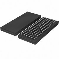
Philips Semiconductors 12. Package outline LFBGA96: plastic low profile fine-pitch ball grid array package; 96 balls; body 13.5 x 5.5 x 1.05 mm ball A1 index area ...
Page 24
Philips Semiconductors 13. Soldering 13.1 Introduction to soldering surface mount packages This text gives a very brief insight to a complex technology. A more in-depth account of soldering ICs can be found in our Data Handbook IC26; Integrated Circuit Packages ...
Page 25
Philips Semiconductors – smaller than 1.27 mm, the footprint longitudinal axis must be parallel to the transport direction of the printed-circuit board. The footprint must incorporate solder thieves at the downstream end. • For packages with leads on four sides, ...
Page 26
Philips Semiconductors [4] These packages are not suitable for wave soldering. On versions with the heatsink on the bottom side, the solder cannot penetrate between the printed-circuit board and the heatsink. On versions with the heatsink on the top side, ...
Page 27
Philips Semiconductors 16. Data sheet status [1] Level Data sheet status Product status I Objective data Development II Preliminary data Qualification III Product data Production [1] Please consult the most recently issued data sheet before initiating or completing a design. ...
Page 28
Philips Semiconductors 21. Contents 1 General description . . . . . . . . . . . . . . . . . . . . . . 1 2 Features . . . . . . . . ...