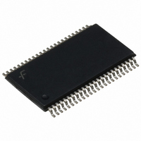
74VCX163245MTD Fairchild Semiconductor, 74VCX163245MTD Datasheet - Page 3

74VCX163245MTD
Manufacturer Part Number
74VCX163245MTD
Description
IC TRANSCVR 16BIT N-INV 48TSSOP
Manufacturer
Fairchild Semiconductor
Series
74VCXr
Datasheet
1.74VCX163245MTDX.pdf
(12 pages)
Specifications of 74VCX163245MTD
Logic Function
Translator, 3-State
Number Of Bits
8
Input Type
Voltage
Output Type
Voltage
Number Of Channels
2
Number Of Outputs/channel
8
Differential - Input:output
No/No
Propagation Delay (max)
4.4ns
Voltage - Supply
1.65 V ~ 3.6 V
Operating Temperature
-40°C ~ 85°C
Package / Case
48-TSSOP
Supply Voltage
*
Logic Type
CMOS
Logic Family
74VCX
Number Of Channels Per Chip
16
Input Level
CMOS
Output Level
CMOS
High Level Output Current
- 24 mA
Low Level Output Current
24 mA
Propagation Delay Time
6.2 ns
Supply Voltage (max)
2.7 V, 3.6 V
Supply Voltage (min)
1.65 V, 2.3 V
Maximum Operating Temperature
+ 85 C
Function
Transceiver
Input Bias Current (max)
20 uA
Minimum Operating Temperature
- 40 C
Mounting Style
SMD/SMT
Number Of Circuits
2
Polarity
Non-Inverting
Lead Free Status / RoHS Status
Lead free / RoHS Compliant
Data Rate
-
Lead Free Status / Rohs Status
Lead free / RoHS Compliant
Available stocks
Company
Part Number
Manufacturer
Quantity
Price
Part Number:
74VCX163245MTDX
Manufacturer:
FAIRCHILD/仙童
Quantity:
20 000
©2000 Fairchild Semiconductor Corporation
74VCX163245 Rev. 1.7
Truth Tables
H
L
X
Z
VCX163245 Translator Power Up Sequence Recommendations
To guard against power up problems, some simple
guidelines need to be adhered to. The VCX163245 is
designed so that the control pins (T/R
plied by V
begin by powering up the control side of the device,
V
ahead of V
and oscillations as all A Port and B Port outputs will be
disabled. To ensure the high impedance state during
power up or power down, OE
through a pull up resistor. The minimum value of the
resistor is determined by the current sourcing capability
of the driver. Second, the T/R
Logic Diagrams
Please note that these diagrams are provided only for the understanding of logic operations and should not be used
to estimate propagation delays.
CCB
OE
LOW Voltage Level
High Impedance
H
Immaterial (HIGH or LOW, inputs may not float)
HIGH Voltage Level
L
L
. The OE
Inputs
1
CCB
CCB
T/R
H
X
L
. Therefore the first recommendation is to
n
, this will guard against bus contentions
1
control pins should be ramped with or
Bus B
Bus A
HIGH Z State on A
0
0
–B
–A
7
7
n
n
Data to Bus A
Data to Bus B
should be tied to V
Outputs
control pins should be
0
n
–A
, OE
7
, B
n
0
0
) are sup-
–A
–B
0
–B
7
7
7
CCB
3
placed at logic LOW (0V) level, this will ensure that the
B-side bus pins are configured as inputs to help guard
against bus contention and oscillations. B-side Data
Inputs should be driven to a valid logic level (0V or
V
lations. V
ever V
ensure proper device operation. Upon completion of
these steps the device can then be configured for the
users desired operation. Following these steps will help
to prevent possible damage to the translator device as
well as other system components.
CCB
OE
H
L
L
Inputs
), this will prevent excessive current draw and oscil-
2
CCA
CCA
T/R
H
must be greater than or equal to V
L
X
can then be powered up after V
2
Bus B
Bus A
HIGH-Z State on A
8
8
–B
–A
15
15
Data to Bus A
Data to Bus B
Outputs
8
–A
15
, B
www.fairchildsemi.com
8
8
–A
–B
8
–B
CCB
15
15
15
CCB
, how-
to


