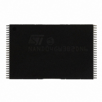
NAND04GW3B2DN6E NUMONYX, NAND04GW3B2DN6E Datasheet - Page 36

NAND04GW3B2DN6E
Manufacturer Part Number
NAND04GW3B2DN6E
Description
IC FLASH 4GBIT 48TSOP
Manufacturer
NUMONYX
Datasheet
1.NAND04GW3B2DN6E.pdf
(72 pages)
Specifications of NAND04GW3B2DN6E
Format - Memory
FLASH
Memory Type
FLASH - Nand
Memory Size
4G (512M x 8)
Interface
Parallel
Voltage - Supply
2.7 V ~ 3.6 V
Operating Temperature
-40°C ~ 85°C
Package / Case
48-TSOP
Lead Free Status / RoHS Status
Lead free / RoHS Compliant
Speed
-
Lead Free Status / RoHS Status
Lead free / RoHS Compliant
Available stocks
Company
Part Number
Manufacturer
Quantity
Price
Company:
Part Number:
NAND04GW3B2DN6E
Manufacturer:
StarMicro
Quantity:
872
Company:
Part Number:
NAND04GW3B2DN6E
Manufacturer:
ST
Quantity:
5 645
Part Number:
NAND04GW3B2DN6E
Manufacturer:
ST
Quantity:
20 000
Device operations
Table 13.
6.10
6.11
6.11.1
36/72
2nd 264-word EDC unit
3rd 264-word EDC unit
1st 264-word EDC unit
4th 264-word EDC unit
EDC unit
Address definition for EDC units (x16 devices)
Reset
The Reset command is used to reset the command interface and status register. If the
Reset command is issued during any operation, the operation is aborted. If the aborted
operation is a program or erase, the contents of the memory locations being modified are no
longer valid as the data is partially programmed or erased.
If the device has already been reset, then the new Reset command is not accepted.
The Ready/Busy signal goes Low for t
of t
issued. Refer to
Read status register
The devices contain a status register that provides information on the current or previous
program or erase operation. The various bits in the status register convey information and
errors on the operation.
The status register is read by issuing the Read Status Register command. The status
register information is present on the output data bus (I/O0-I/O7) on the falling edge of Chip
Enable or Read Enable, whichever occurs last. When several memories are connected in a
system, the use of Chip Enable and Read Enable signals allows the system to poll each
device separately, even when the Ready/Busy pins are common-wired. It is not necessary to
toggle the Chip Enable or Read Enable signals to update the contents of the status register.
After the Read Status Register command has been issued, the device remains in read
status register mode until another command is issued. Therefore, if a Read Status Register
command is issued during a random read cycle, a new Read command must be issued to
continue with a page read operation.
The status register bits are summarized in
conjunction with the following sections.
Write protection bit (SR7)
The write protection bit identifies if the device is protected or not. If the write protection bit is
set to ‘1’, the device is not protected and program or erase operations are allowed. If the
write protection bit is set to ‘0’ the device is protected and program or erase operations are
not allowed.
BLBH4
depends on the operation that the device was performing when the command was
Area name
Table 31
C
D
A
B
for the values.
Main area
Column address
768 to 1023
256 to 511
512 to 767
0 to 255
BLBH4
Table 14: Status register
after the Reset command is issued. The value
Area name
NAND04G-B2D, NAND08G-BxC
G
H
E
F
Spare area
bits. Refer to
Column address
1024 to 1031
1032 to 1039
1040 to 1047
1048 to 1055
Table 14
in


