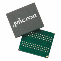
MT48H8M32LFB5-10 IT Micron Technology Inc, MT48H8M32LFB5-10 IT Datasheet - Page 22

MT48H8M32LFB5-10 IT
Manufacturer Part Number
MT48H8M32LFB5-10 IT
Description
IC SDRAM 256MBIT 100MHZ 90VFBGA
Manufacturer
Micron Technology Inc
Type
Mobile SDRAMr
Specifications of MT48H8M32LFB5-10 IT
Format - Memory
RAM
Memory Type
Mobile SDRAM
Memory Size
256M (8Mx32)
Speed
100MHz
Interface
Parallel
Voltage - Supply
1.7 V ~ 1.95 V
Operating Temperature
-40°C ~ 85°C
Package / Case
90-VFBGA
Organization
8Mx32
Density
256Mb
Address Bus
14b
Access Time (max)
17/8/7ns
Maximum Clock Rate
104MHz
Operating Supply Voltage (typ)
1.8V
Package Type
VFBGA
Operating Temp Range
-40C to 85C
Operating Supply Voltage (max)
1.9V
Operating Supply Voltage (min)
1.7V
Supply Current
65mA
Pin Count
90
Mounting
Surface Mount
Operating Temperature Classification
Industrial
Lead Free Status / RoHS Status
Lead free / RoHS Compliant
WRITEs
as shown in Figure 16.
vided with the WRITE command, and auto precharge
is either enabled or disabled for that access. If auto
precharge is enabled, the row being accessed is pre-
charged at the completion of the burst. For the generic
WRITE commands used in the following illustrations,
auto precharge is disabled.
will be registered coincident with the WRITE com-
mand. Subsequent data elements will be registered on
each successive positive clock edge. Upon completion
of a fixed-length burst, assuming no other commands
have been initiated, the DQs will remain High-Z and
any additional input data will be ignored (see Figure
17). A full-page burst will continue until terminated.
(At the end of the page, it will wrap to column 0 and
continue.)
pdf: 09005aef80d460f2, source: 09005aef80cd8d41
256Mb SDRAM x32_2.fm - Rev. D 9/04 EN
WRITE bursts are initiated with a WRITE command,
The starting column and bank addresses are pro-
During WRITE bursts, the first valid data-in element
A9, A11
A0-A8
BA0,1
RAS#
CAS#
Figure 16: WRITE Command
WE#
CKE
A10
CLK
CS#
HIGH
VALID ADDRESS
DISABLE AUTO PRECHARGE
ENABLE AUTO PRECHARGE
ADDRESS
ADDRESS
COLUMN
BANK
DON’T CARE
22
subsequent WRITE command, and data for a fixed-
length WRITE burst may be immediately followed by
data for a WRITE command. The new WRITE com-
mand can be issued on any clock following the previ-
ous WRITE command, and the data provided
coincident with the new command applies to the new
command. An example is shown in Figure 18. Data n +
1 is either the last of a burst of two or the last desired of
a longer burst. The 256Mb SDRAM uses a pipelined
architecture and therefore does not require the 2n rule
associated with a prefetch architecture. A WRITE com-
mand can be initiated on any clock cycle following a
previous WRITE command. Full-speed random write
accesses within a page can be performed to the same
bank, as shown in Figure 19, or each subsequent
WRITE may be performed to a different bank.
Data for any WRITE burst may be truncated with a
COMMAND
ADDRESS
Micron Technology, Inc., reserves the right to change products or specifications without notice.
NOTE:
Figure 18: WRITE to WRITE
COMMAND
CLK
DQ
ADDRESS
Figure 17: WRITE Burst
NOTE:
Burst length = 2. DQM is LOW.
CLK
DQ
WRITE
BANK,
COL n
T0
D
n
IN
DQM is LOW. Each WRITE
command may be to any bank.
WRITE
BANK,
COL n
D
T0
n
IN
NOP
n + 1
T1
D
MOBILE SDRAM
IN
©2003 Micron Technology, Inc. All rights reserved.
n + 1
NOP
T1
D
IN
DON’T CARE
256Mb: x32
NOP
T2
PRELIMINARY
WRITE
BANK,
COL b
DON’T CARE
T2
D
b
IN
T3
NOP


