ICE3BR0665JF Infineon Technologies, ICE3BR0665JF Datasheet - Page 34
ICE3BR0665JF
Manufacturer Part Number
ICE3BR0665JF
Description
IC OFFLINE CTLR SMPS OTP TO220-6
Manufacturer
Infineon Technologies
Series
CoolSET®F3Rr
Type
Off Line Switcherr
Specifications of ICE3BR0665JF
Output Isolation
Isolated
Frequency Range
58 ~ 75kHz
Voltage - Input
10.5 ~ 27 V
Voltage - Output
650V
Power (watts)
42W
Operating Temperature
-25°C ~ 130°C
Package / Case
TO-220-6 Formed Leads
Output Voltage
650 V
Input / Supply Voltage (max)
27 V
Input / Supply Voltage (min)
- 0.3 V
Duty Cycle (max)
75 %
Switching Frequency
67 KHz
Operating Temperature Range
- 25 C to + 130 C
Mounting Style
Through Hole
Maximum Operating Temperature
+ 130 C
Minimum Operating Temperature
- 25 C
Output Power
259 W
Lead Free Status / RoHS Status
Lead free / RoHS Compliant
Other names
SP000366360
Available stocks
Company
Part Number
Manufacturer
Quantity
Price
Company:

Part Number:
ICE3BR0665JF
Manufacturer:
INFINEON
Quantity:
3 400


10
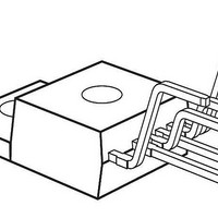
Figure 72
General guideline for PCB layout design using F3/F3R CoolSET (refer to Figure 72):
1. “Star Ground “at bulk capacitor ground, C11:
Guideline for PCB layout design when >3KV lightning surge test applied (refer to Figure 72):
1. Add spark gap
Version 2.0
2. High voltage traces clearance:
3. Filter capacitor close to the controller ground:
a. Spark Gap 3 and Spark Gap 4, input common mode choke, L1:
a. 400V traces (positive rail of bulk capacitor C11) to nearby trace: > 2.0mm
b. 600V traces (drain voltage of CoolSET IC11) to nearby trace: > 2.5mm
a. DC ground of the primary auxiliary winding in power transformer, TR1, and ground of C16 and Z11.
b. DC ground of the current sense resistor, R12
c. DC ground of the CoolSET device, GND pin of IC11; the signal grounds from C13, C14, C15 and collector of
d. DC ground from bridge rectifier, BR1
e. DC ground from the bridging Y-capacitor, C4
High voltage traces should keep enough spacing to the nearby traces. Otherwise, arcing would incur.
Spark Gap 1
Spark Gap 2
Spark gap is a pair of saw-tooth like copper plate facing each other which can discharge the accumulated
Gap separation is around 1.5mm (no safety concern)
charge during surge test through the sharp point of the saw-tooth plate.
Filter capacitors, C13, C14 and C15 should be placed as close to the controller ground and the controller pin
as possible so as to reduce the switching noise coupled into the controller.
“Star Ground “means all primary DC grounds should be connected to the ground of bulk capacitor C11
separately in one point. It can reduce the switching noise going into the sensitive pins of the CoolSET device
effectively. The primary DC grounds include the followings.
IC12 should be connected to the GND pin of IC11 and then “star “connect to the bulk capacitor ground.
GND
L
N
FUSE1
Schematic for recommended PCB layout
Y-CAP
Schematic for recommended PCB layout
C2
X-CAP
C1
C3
Y-CAP
Spark Gap 4
Spark Gap 3
F3 CoolSET schematic for recommended PCB layout
L1
C4
Y-CAP
BR1
C11
R12
C13
bulk cap
*
BA
GND
D11
CS
C14
IC11
CoolSET
F3
FB
34
Schematic for recommended PCB layout
C15
DRAIN
VCC
NC
R11
R13
Z11
R14
D11
C16
D13
C12
TR1
IC12
D21
R23
ICE3BR0665JF
CoolSET
C21
R22
C23
IC21
C22
R25
R21
R24
11 Sep 2008
®
-F3R
GND
Vo
Related parts for ICE3BR0665JF
Image
Part Number
Description
Manufacturer
Datasheet
Request
R

Part Number:
Description:
Manufacturer:
Infineon Technologies AG
Datasheet:
Part Number:
Description:
Manufacturer:
Infineon Technologies AG
Datasheet:
Part Number:
Description:
Manufacturer:
Infineon Technologies AG
Datasheet:
Part Number:
Description:
Manufacturer:
Infineon Technologies AG
Datasheet:
Part Number:
Description:
Manufacturer:
Infineon Technologies AG
Datasheet:
Part Number:
Description:
Manufacturer:
Infineon Technologies AG
Datasheet:
Part Number:
Description:
Manufacturer:
Infineon Technologies AG
Datasheet:
Part Number:
Description:
16-bit microcontroller with 2x2 KByte RAM
Manufacturer:
Infineon Technologies AG
Datasheet:
Part Number:
Description:
NPN silicon RF transistor
Manufacturer:
Infineon Technologies AG
Datasheet:
Part Number:
Description:
NPN silicon RF transistor
Manufacturer:
Infineon Technologies AG
Datasheet:
Part Number:
Description:
NPN silicon RF transistor
Manufacturer:
Infineon Technologies AG
Datasheet:
Part Number:
Description:
NPN silicon RF transistor
Manufacturer:
Infineon Technologies AG
Datasheet:
Part Number:
Description:
Si-MMIC-amplifier in SIEGET 25-technologie
Manufacturer:
Infineon Technologies AG
Datasheet:
Part Number:
Description:
IGBT Power Module
Manufacturer:
Infineon Technologies AG
Datasheet:
Part Number:
Description:
IC for switching-mode power supplies
Manufacturer:
Infineon Technologies AG
Datasheet: