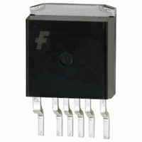
FS6X1220RJ Fairchild Semiconductor, FS6X1220RJ Datasheet - Page 10

FS6X1220RJ
Manufacturer Part Number
FS6X1220RJ
Description
IC SWIT PWM CM OVP UVLO HV D2PAK
Manufacturer
Fairchild Semiconductor
Datasheet
1.FS6X0420RJ.pdf
(15 pages)
Specifications of FS6X1220RJ
Output Isolation
Isolated
Frequency Range
270 ~ 330kHz
Voltage - Input
9 ~ 35 V
Voltage - Output
200V
Power (watts)
36W
Operating Temperature
-25°C ~ 150°C
Package / Case
TO-263-7, D²Pak (6 leads + Tab), TO-263CB
Number Of Outputs
1
Duty Cycle (max)
88 %
Mounting Style
SMD/SMT
Switching Frequency
300 KHz
Operating Supply Voltage
35 V
Maximum Operating Temperature
+ 85 C
Minimum Operating Temperature
- 25 C
Synchronous Pin
No
Topology
Flyback, Forward
Lead Free Status / RoHS Status
Lead free / RoHS Compliant
Available stocks
Company
Part Number
Manufacturer
Quantity
Price
Company:
Part Number:
FS6X1220RJX
Manufacturer:
Fairchild Semiconductor
Quantity:
135
FS6X0420RJ/ FS6X0720RJ/ FS6X1220RJ Rev. 1.0.1
3.2 Over Load Protection (OLP)
Overload means that the load current exceeds a pre-set level
due to an abnormal situation. In this situation, the protection cir-
cuit should be activated to protect the SMPS (Switch Mode
Power Supplies). However, even when the SMPS is in normal
operation, the over load protection circuit can be activated dur-
ing the load transition. To avoid this undesired operation, the
over load protection circuit is designed to be activated after a
specified period to determine whether it is a transient situation
or an overload situation. Because of the pulse-by-pulse current
limit capability, the maximum peak current through the SMPS is
limited, and therefore the maximum input power is restricted
with a given input voltage. If the output consumes beyond this
maximum power, the output voltage (Vo) decreases below the
set voltage. This reduces the current through the opto-coupler
diode which also reduces opto-coupler transistor current
increasing Vfb. If Vfb exceeds 2.6V, D1 is blocked and the 5mA
current source starts to charge Cfb slowly compared to when
the 0.9mA current source charges Cfb. In this condition, Vfb
continues increasing until it reaches 7.5V, and the switching
operation is terminated at that time as shown in Figure 19. The
delay time for shutdown is the time required to charge Cfb from
2.6V to 7.5V with 5mA. When Cfb is 10nF (103), T12 is approxi-
mately 9.8ms and when Cfb is 0.1mF (104), T12 is approxi-
mately 98ms. These values are enough to prevent SMPS from
being shut down during transient situations.
3.3 Over Voltage Protection (OVP)
In the case of a malfunction in the secondary side feedback cir-
cuit, or feedback loop open caused by a defect of solder, the
current through the opto-coupler transistor becomes almost
zero. Then, Vfb climbs up in a similar manner to the over load
situation, forcing the preset maximum current to be supplied to
the secondary side until the over load protection is activated.
Because more than required energy is provided to the output,
the output voltage may exceed the rated voltage before the over
load protection is activated, resulting in the breakdown of the
devices in the secondary side. To prevent this situation, an over
voltage protection (OVP) circuit is employed. In general, Vcc is
proportional to the output voltage and FS6X-Series uses Vcc
instead of directly monitoring the output voltage. If VCC
exceeds 25V, OVP circuit is activated resulting in termination of
7.5V
2.6V
V
FB
Figure 19. Over Load Protection
T
1
T
Over load protection
12
= Cfb*(7.5-2.6)/I
delay
T
2
t
10
switching. To avoid undesired activation of OVP during normal
operation, Vcc should be properly designed to be below 25V.
3.4 Thermal Shutdown (TSD)
The thermal shutdown circuitry senses the junction tempera-
ture. The threshold is set at 160×C. When the junction tempera-
ture rises above this threshold (160×C), the power MOSFET is
disabled.
4. Line UVLO and Sleep Mode
According to the voltage of the Line Sense pin, three operation
modes are defined: normal operation mode, line under voltage
lock out mode, and sleep mode, as shown in Figure 20. When
the voltage of this pin is over 2.55V, FS6X-Series operates in
normal mode. When the voltage of this pin is less than 2.55V, it
goes into line under voltage lock out mode terminating switching
operation. When the voltage of this pin is less than 1.8V, it
enters into sleep mode. During sleep mode, the reference volt-
age generation circuit, including the shunt regulator, is disabled
and only 300mA operation current is required.
ON OFF
Sleep
Figure 20. Line Sense Block
Vin
R2
R1
Sense
Line
6
(2.5V)
(1.8v)
V
V
SL
LU
Vcc good
Line UVLO
Enable
www.fairchildsemi.com
Internal
Bias
Vref
9V/15V
3
Vcc


