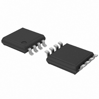
PCA9550DP,118 NXP Semiconductors, PCA9550DP,118 Datasheet - Page 15

PCA9550DP,118
Manufacturer Part Number
PCA9550DP,118
Description
IC LED DRIVER BLINKER 8-TSSOP
Manufacturer
NXP Semiconductors
Type
LED Blinkerr
Datasheet
1.PCA9550DP118.pdf
(26 pages)
Specifications of PCA9550DP,118
Package / Case
8-TSSOP
Topology
Open Drain, PWM
Number Of Outputs
2
Internal Driver
Yes
Type - Primary
LED Blinker
Frequency
400kHz
Voltage - Supply
2.3 V ~ 5.5 V
Mounting Type
Surface Mount
Operating Temperature
-40°C ~ 85°C
Current - Output / Channel
25mA
Internal Switch(s)
Yes
Low Level Output Current
6.5 mA
Operating Supply Voltage
2.3 V to 5.5 V
Maximum Supply Current
500 uA
Maximum Power Dissipation
400 mW
Maximum Operating Temperature
+ 85 C
Mounting Style
SMD/SMT
Minimum Operating Temperature
- 40 C
Operating Supply Voltage (typ)
2.5/3.3/5V
Number Of Segments
2
Operating Temperature (min)
-40C
Operating Temperature (max)
85C
Operating Temperature Classification
Industrial
Package Type
TSSOP
Pin Count
8
Mounting
Surface Mount
Power Dissipation
400mW
Operating Supply Voltage (min)
2.3V
Operating Supply Voltage (max)
5.5V
Lead Free Status / RoHS Status
Lead free / RoHS Compliant
For Use With
OM6285 - EVAL BOARD I2C-2002-1A568-4002 - DEMO BOARD I2C
Voltage - Output
-
Efficiency
-
Lead Free Status / Rohs Status
Lead free / RoHS Compliant
Other names
568-3387-2
935272881118
PCA9550DP-T
935272881118
PCA9550DP-T
NXP Semiconductors
11. Dynamic characteristics
Table 14.
[1]
[2]
[3]
[4]
[5]
PCA9550_5
Product data sheet
Symbol
f
t
t
t
t
t
t
t
t
t
t
t
t
t
Port timing
t
t
t
Reset
t
t
t
SCL
BUF
HD;STA
SU;STA
SU;STO
HD;DAT
VD;ACK
VD;DAT
SU;DAT
LOW
HIGH
r
f
SP
v(Q)
su(D)
h(D)
w(rst)
rec(rst)
rst
t
t
C
Resetting the device while actively communicating on the bus may cause glitches or errant STOP conditions.
Upon reset, the full delay will be the sum of t
VD;ACK
VD;DAT
b
= total capacitance of one bus line in pF.
= minimum time for SDA data output to be valid following SCL LOW.
= time for Acknowledgement signal from SCL LOW to SDA (out) LOW.
Dynamic characteristics
Parameter
SCL clock frequency
bus free time between a STOP and
START condition
hold time (repeated) START condition
set-up time for a repeated START
condition
set-up time for STOP condition
data hold time
data valid acknowledge time
data valid time
data set-up time
LOW period of the SCL clock
HIGH period of the SCL clock
rise time of both SDA and SCL signals
fall time of both SDA and SCL signals
pulse width of spikes that must be
suppressed by the input filter
data output valid time
data input set-up time
data input hold time
reset pulse width
reset recovery time
reset time
rst
and the RC time constant of the SDA bus.
Rev. 05 — 13 October 2008
Conditions
LOW-level
HIGH-level
2-bit I
2
C-bus LED driver with programmable blink rates
[4][5]
[1]
[2]
[2]
Standard-mode
Min
250
100
400
4.7
4.0
4.7
4.0
4.7
4.0
0
0
1
6
0
-
-
-
-
-
-
-
I
2
C-bus
1500
1000
Max
100
600
600
300
200
50
-
-
-
-
-
-
-
-
-
-
-
-
-
20 + 0.1C
20 + 0.1C
Fast-mode I
Min
100
100
400
1.3
0.6
0.6
0.6
1.3
0.6
0
0
1
6
0
-
-
-
-
-
PCA9550
b
b
© NXP B.V. 2008. All rights reserved.
[3]
[3]
2
C-bus
Max
400
600
600
600
300
300
200
50
-
-
-
-
-
-
-
-
-
-
-
-
-
15 of 26
Unit
kHz
ns
ns
ns
ns
ns
ns
ns
ns
ns
ns
ns
ns
ns
s
s
s
s
s
s
s


