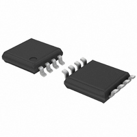
PCA9550DP,118 NXP Semiconductors, PCA9550DP,118 Datasheet - Page 4

PCA9550DP,118
Manufacturer Part Number
PCA9550DP,118
Description
IC LED DRIVER BLINKER 8-TSSOP
Manufacturer
NXP Semiconductors
Type
LED Blinkerr
Datasheet
1.PCA9550DP118.pdf
(26 pages)
Specifications of PCA9550DP,118
Package / Case
8-TSSOP
Topology
Open Drain, PWM
Number Of Outputs
2
Internal Driver
Yes
Type - Primary
LED Blinker
Frequency
400kHz
Voltage - Supply
2.3 V ~ 5.5 V
Mounting Type
Surface Mount
Operating Temperature
-40°C ~ 85°C
Current - Output / Channel
25mA
Internal Switch(s)
Yes
Low Level Output Current
6.5 mA
Operating Supply Voltage
2.3 V to 5.5 V
Maximum Supply Current
500 uA
Maximum Power Dissipation
400 mW
Maximum Operating Temperature
+ 85 C
Mounting Style
SMD/SMT
Minimum Operating Temperature
- 40 C
Operating Supply Voltage (typ)
2.5/3.3/5V
Number Of Segments
2
Operating Temperature (min)
-40C
Operating Temperature (max)
85C
Operating Temperature Classification
Industrial
Package Type
TSSOP
Pin Count
8
Mounting
Surface Mount
Power Dissipation
400mW
Operating Supply Voltage (min)
2.3V
Operating Supply Voltage (max)
5.5V
Lead Free Status / RoHS Status
Lead free / RoHS Compliant
For Use With
OM6285 - EVAL BOARD I2C-2002-1A568-4002 - DEMO BOARD I2C
Voltage - Output
-
Efficiency
-
Lead Free Status / Rohs Status
Lead free / RoHS Compliant
Other names
568-3387-2
935272881118
PCA9550DP-T
935272881118
PCA9550DP-T
NXP Semiconductors
6. Functional description
PCA9550_5
Product data sheet
6.1 Device address
6.2 Control register
Refer to
Following a START condition, the bus master must output the address of the slave it is
accessing. The address of the PCA9550 is shown in
internal pull-up resistor is incorporated on the hardware selectable address pin and it must
be pulled HIGH or LOW.
The last bit of the address byte defines the operation to be performed. When set to logic 1
a read is selected, while a logic 0 selects a write operation.
Following the successful acknowledgement of the slave address, the bus master will send
a byte to the PCA9550, which will be stored in the Control register.
The lowest 3 bits are used as a pointer to determine which register will be accessed.
If the Auto-Increment (AI) flag is set, the three low order bits of the Control register are
automatically incremented after a read or write. This allows the user to program the
registers sequentially. The contents of these bits will rollover to ‘000’ after the last register
is accessed.
When the Auto-Increment flag is set (AI = 1) and a read sequence is initiated, the
sequence must start by reading a register different from the input register
(B2 B1 B0
Only the 3 least significant bits are affected by the AI flag. Unused bits must be
programmed with zeroes.
Fig 5.
Fig 6.
Figure 1 “Block diagram of
PCA9550 slave address
Reset state: 00h
Control register
000).
Rev. 05 — 13 October 2008
Auto-Increment flag
2-bit I
1
0
1
0
PCA9550”.
2
C-bus LED driver with programmable blink rates
slave address
0
0
fixed
AI
0
0
0
register address
B2
0
selectable
hardware
Figure
A0 R/W
002aad242
B1
002aad243
B0
5. To conserve power, no
PCA9550
© NXP B.V. 2008. All rights reserved.
4 of 26


