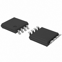
PCA9550DP,118 NXP Semiconductors, PCA9550DP,118 Datasheet - Page 5

PCA9550DP,118
Manufacturer Part Number
PCA9550DP,118
Description
IC LED DRIVER BLINKER 8-TSSOP
Manufacturer
NXP Semiconductors
Type
LED Blinkerr
Datasheet
1.PCA9550DP118.pdf
(26 pages)
Specifications of PCA9550DP,118
Package / Case
8-TSSOP
Topology
Open Drain, PWM
Number Of Outputs
2
Internal Driver
Yes
Type - Primary
LED Blinker
Frequency
400kHz
Voltage - Supply
2.3 V ~ 5.5 V
Mounting Type
Surface Mount
Operating Temperature
-40°C ~ 85°C
Current - Output / Channel
25mA
Internal Switch(s)
Yes
Low Level Output Current
6.5 mA
Operating Supply Voltage
2.3 V to 5.5 V
Maximum Supply Current
500 uA
Maximum Power Dissipation
400 mW
Maximum Operating Temperature
+ 85 C
Mounting Style
SMD/SMT
Minimum Operating Temperature
- 40 C
Operating Supply Voltage (typ)
2.5/3.3/5V
Number Of Segments
2
Operating Temperature (min)
-40C
Operating Temperature (max)
85C
Operating Temperature Classification
Industrial
Package Type
TSSOP
Pin Count
8
Mounting
Surface Mount
Power Dissipation
400mW
Operating Supply Voltage (min)
2.3V
Operating Supply Voltage (max)
5.5V
Lead Free Status / RoHS Status
Lead free / RoHS Compliant
For Use With
OM6285 - EVAL BOARD I2C-2002-1A568-4002 - DEMO BOARD I2C
Voltage - Output
-
Efficiency
-
Lead Free Status / Rohs Status
Lead free / RoHS Compliant
Other names
568-3387-2
935272881118
PCA9550DP-T
935272881118
PCA9550DP-T
NXP Semiconductors
PCA9550_5
Product data sheet
6.2.1 Control register definition
6.3.1 INPUT - Input register
6.3.2 PSC0 - Frequency Prescaler 0
6.3.3 PWM0 - Pulse Width Modulation 0
6.3 Register descriptions
Table 4.
The INPUT register reflects the state of the device pins. Writes to this register will be
acknowledged but will have no effect.
Table 5.
Remark: The default value ‘X’ is determined by the externally applied logic level (normally
logic 1) when used for directly driving LED with pull-up to V
PSC0 is used to program the period of the PWM output.
The period of BLINK0 = (PSC0 + 1) / 44.
Table 6.
The PWM0 register determines the duty cycle of BLINK0. The outputs are LOW (LED off)
when the count is less than the value in PWM0 and HIGH when it is greater. If PWM0 is
programmed with 00h, then the PWM0 output is always LOW.
The duty cycle of BLINK0 = (256
Table 7.
B2
0
0
0
0
1
1
Bit
Symbol
Default
Bit
Symbol
Default
Bit
Symbol
Default
B1
0
0
1
1
0
0
Register summary
INPUT - Input register description
PSC0 - Frequency Prescaler 0 register description
PSC0[7]
PWM0 - Pulse Width Modulation 0 register description
PWM0
[7]
7
0
7
1
7
1
B0
0
1
0
1
0
1
PSC0[6]
Register name
INPUT
PSC0
PWM0
PSC1
PWM1
LS0
PWM0
Rev. 05 — 13 October 2008
[6]
6
0
6
1
6
0
2-bit I
PSC0[5]
PWM0
[5]
5
0
5
1
5
0
PWM0) / 256.
not used
2
C-bus LED driver with programmable blink rates
PSC0[4]
PWM0
Access
read only
read/write
read/write
read/write
read/write
read/write
[4]
4
0
4
1
4
0
PSC0[3]
PWM0
[3]
3
0
3
1
3
0
Description
input register
frequency prescaler 0
PWM register 0
frequency prescaler 1
PWM register 1
LED selector
DD
PSC0[2]
PWM0
.
[2]
2
2
2
0
0
1
PCA9550
PSC0[1]
© NXP B.V. 2008. All rights reserved.
PWM0
LED1
[1]
X
1
1
1
1
0
PSC0[0]
PWM0
LED0
[0]
X
0
0
1
0
0
5 of 26


