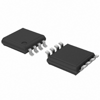
PCA9550DP,118 NXP Semiconductors, PCA9550DP,118 Datasheet - Page 22

PCA9550DP,118
Manufacturer Part Number
PCA9550DP,118
Description
IC LED DRIVER BLINKER 8-TSSOP
Manufacturer
NXP Semiconductors
Type
LED Blinkerr
Datasheet
1.PCA9550DP118.pdf
(26 pages)
Specifications of PCA9550DP,118
Package / Case
8-TSSOP
Topology
Open Drain, PWM
Number Of Outputs
2
Internal Driver
Yes
Type - Primary
LED Blinker
Frequency
400kHz
Voltage - Supply
2.3 V ~ 5.5 V
Mounting Type
Surface Mount
Operating Temperature
-40°C ~ 85°C
Current - Output / Channel
25mA
Internal Switch(s)
Yes
Low Level Output Current
6.5 mA
Operating Supply Voltage
2.3 V to 5.5 V
Maximum Supply Current
500 uA
Maximum Power Dissipation
400 mW
Maximum Operating Temperature
+ 85 C
Mounting Style
SMD/SMT
Minimum Operating Temperature
- 40 C
Operating Supply Voltage (typ)
2.5/3.3/5V
Number Of Segments
2
Operating Temperature (min)
-40C
Operating Temperature (max)
85C
Operating Temperature Classification
Industrial
Package Type
TSSOP
Pin Count
8
Mounting
Surface Mount
Power Dissipation
400mW
Operating Supply Voltage (min)
2.3V
Operating Supply Voltage (max)
5.5V
Lead Free Status / RoHS Status
Lead free / RoHS Compliant
For Use With
OM6285 - EVAL BOARD I2C-2002-1A568-4002 - DEMO BOARD I2C
Voltage - Output
-
Efficiency
-
Lead Free Status / Rohs Status
Lead free / RoHS Compliant
Other names
568-3387-2
935272881118
PCA9550DP-T
935272881118
PCA9550DP-T
NXP Semiconductors
PCA9550_5
Product data sheet
15.4 Reflow soldering
Key characteristics in reflow soldering are:
Table 15.
Table 16.
Moisture sensitivity precautions, as indicated on the packing, must be respected at all
times.
Studies have shown that small packages reach higher temperatures during reflow
soldering, see
Package thickness (mm)
< 2.5
Package thickness (mm)
< 1.6
1.6 to 2.5
> 2.5
•
•
•
•
•
2.5
Process issues, such as application of adhesive and flux, clinching of leads, board
transport, the solder wave parameters, and the time during which components are
exposed to the wave
Solder bath specifications, including temperature and impurities
Lead-free versus SnPb soldering; note that a lead-free reflow process usually leads to
higher minimum peak temperatures (see
reducing the process window
Solder paste printing issues including smearing, release, and adjusting the process
window for a mix of large and small components on one board
Reflow temperature profile; this profile includes preheat, reflow (in which the board is
heated to the peak temperature) and cooling down. It is imperative that the peak
temperature is high enough for the solder to make reliable solder joints (a solder paste
characteristic). In addition, the peak temperature must be low enough that the
packages and/or boards are not damaged. The peak temperature of the package
depends on package thickness and volume and is classified in accordance with
Table 15
SnPb eutectic process (from J-STD-020C)
Lead-free process (from J-STD-020C)
and
Figure
16
26.
Rev. 05 — 13 October 2008
Package reflow temperature ( C)
Volume (mm
< 350
235
220
Package reflow temperature ( C)
Volume (mm
< 350
260
260
250
2-bit I
2
C-bus LED driver with programmable blink rates
3
3
)
)
Figure
350 to 2000
260
250
245
26) than a SnPb process, thus
220
220
350
> 2000
260
245
245
PCA9550
© NXP B.V. 2008. All rights reserved.
22 of 26


