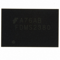
FDMS2380 Fairchild Semiconductor, FDMS2380 Datasheet - Page 4

FDMS2380
Manufacturer Part Number
FDMS2380
Description
IC SOLENOID DRIVER DUAL 18QFN
Manufacturer
Fairchild Semiconductor
Type
Low Sider
Datasheet
1.FDMS2380.pdf
(15 pages)
Specifications of FDMS2380
Input Type
Non-Inverting
Number Of Outputs
2
On-state Resistance
30 mOhm
Current - Output / Channel
5A
Voltage - Supply
6 V ~ 26 V
Operating Temperature
-40°C ~ 160°C
Mounting Type
Surface Mount
Package / Case
18-FQFN
Lead Free Status / RoHS Status
Lead free / RoHS Compliant
Current - Peak Output
-
Other names
FDMS2380TR
Available stocks
Company
Part Number
Manufacturer
Quantity
Price
Part Number:
FDMS2380
Manufacturer:
FAIRCHILD/仙童
Quantity:
20 000
FDMS2380 Rev. A
Electrical Characteristics
Off Characteristics
On Characteristics
Switching Characteristics
Logic Input Characteristics
Protection and Diagnostics Characteristics
Notes:
1. Integrated protection functions, as described in this data sheet, are designed to prevent the destruction of the IC and these fault conditions are considered ‘outside’
the normal operating ranges. It is important to note that the protection functions integrated into this device are NOT designed for continuous repetitive operation.
V
I
I
r
V
t
t
t
t
V
V
V
I
T
I
V
V
I
V
R
T
V
V
V
td
t
t
V
V
SQ
LK
d(ON)
d(OFF)
r
f
IN
OUT(trip)
OUT(ol)
DAIGFB
DIAG(prot)
DS(ON)
J(tsd)
SS
BATT(Oper)
Recir(sat)
IL
IH
CL
BATT(ov)
BATT(uv)
OUT(SS)
OUT(cl1)
OUT(cl2)
FB
DIAG(low)
DIAG(cl)
Symbol
SS
(DIAG)
(min)
Operating Supply Voltage
Supply Quiescent Current
Output Leakage Current
On Resistance - Excitation Path
Saturation Voltage - Recirculation
Path
Output Turn-On Delay Time
Output Turn-Off Delay Time
Rise Time
Fall Time
Input Low Level Voltage
Input High Level Voltage
Input Clamp Voltage
Input Current (each input)
Thermal Shut-down Junction
Temperature
Output Current Trip
Over-voltage Threshold
Under-voltage Threshold
Open Load Detect Current
Soft Short Detect Voltage
Soft Short Resistance
Soft Short Active Time
NDMOS Over-voltage Clamp
Output Inductive Clamp Voltage
Flyback Diagnostic Threshold
Voltage (V
Diagnostic Propagation Delay Time
Minimum Diagnostic Flyback Time
Protection Diagnostic Pulse Width
Diagnostic Voltage Low
Diagnostic Output Clamp Voltage
OUT
Parameter
− V
BATT
(Excitation Path)
)
T
C
= 25°C unless otherwise noted
V
V
V
I
V
V
V
I
V
V
V
INA=0, INB=1, V
INA=0, INB=1, from V
INA=0, INB=1, time R
Ref to GND; I
V
Threshold where DIAG goes low
during Fast turn-off Mode
Fast turn-off Mode; V
Over-voltage, Under-voltage,
Over-current, Over-temperature
I
Diagnostic output active
I
OUT
IN
DIAG
DIAG
BATT
BATT
BATT
BATT
INB
BATT
INA
INA
INA
OUT
<=10mA
= 5A
= 0V, I
= V
= V
= 5V, V
<= 1mA,
<= 10mA
− V
= 13V, V
= 18V, V
= 13V, V
= 13V, V
= 14V, R
(Note 1)
INB
INB
Test Conditions
4
BATT
OUT
= 5V
= 1.5V
INB
; I
OUT
INA
INA
INA
INA
Load
= 10A
= falling edge
OUT
---
---
---
---
---
---
---
---
BATT
T
= V
= V
= V
= 5V,
= 5A
C
= 2.5Ω
= 5A
DIAG
= 150
− V
OUT
SS
INB
INB
INB
is active
OUT
= 5V
= 1.5V
= 5V,
to V
= 1V
o
C
BATT
Min
160
300
6.0
3.5
5.5
0.3
5.5
20
15
27
50
60
27
22
26
1
2
-
-
-
-
-
-
-
-
-
-
-
-
-
-
0.030
0.050
14.0
0.43
Typ
172
450
9.3
0.2
1.4
7.0
8.3
6.5
3.0
5.1
90
60
20
29
75
73
30
23
42
3
7
-
-
-
-
-
-
www.fairchildsemi.com
0.080
0.100
Max
26.0
160
185
800
140
1.8
1.5
5.5
0.6
0.9
15
30
30
10
10
30
32
85
33
33
10
50
10
5
3
-
-
-
-
Units
mA
mA
mA
ms
μA
μA
o
μs
μs
μs
μs
μs
μs
μs
Ω
Ω
Ω
V
V
V
V
V
A
V
V
V
V
V
V
V
V
C


