TCA3727 Infineon Technologies, TCA3727 Datasheet - Page 22
TCA3727
Manufacturer Part Number
TCA3727
Description
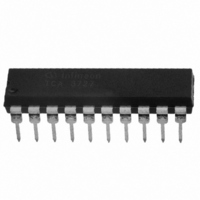
IC DRIVER STEPPER MOTOR DIP-20
Manufacturer
Infineon Technologies
Type
Stepper Motor Controller/Driverr
Datasheet
1.TCA3727.pdf
(29 pages)
Specifications of TCA3727
Applications
Stepper Motor Driver, 2 Phase
Number Of Outputs
2
Current - Output
750mA
Voltage - Supply
5 V ~ 50 V
Operating Temperature
-40°C ~ 110°C
Mounting Type
Through Hole
Package / Case
20-DIP (0.300", 7.62mm)
Product
Stepper Motor Controllers / Drivers
Operating Supply Voltage
5 V to 50 V
Supply Current
2 A
Mounting Style
Through Hole
Lead Free Status / RoHS Status
Contains lead / RoHS non-compliant
Voltage - Load
-
Lead Free Status / Rohs Status
Lead free / RoHS Compliant
Other names
SP000011713
TCA3727
TCA3727IN
TCA3727NK
TCA3727
TCA3727IN
TCA3727NK
Available stocks
Company
Part Number
Manufacturer
Quantity
Price
Company:

Part Number:
TCA3727
Manufacturer:
SIEMENS
Quantity:
5 510
Company:
Part Number:
TCA3727G
Manufacturer:
Yaskawa
Quantity:
100
Company:
Part Number:
TCA3727G
Manufacturer:
SIEMENS
Quantity:
5 510
Part Number:
TCA3727G
Manufacturer:
INFTEL
Quantity:
20 000
Part Number:
TCA3727G-P
Manufacturer:
INF
Quantity:
20 000


Calculation of Power Dissipation
The total power dissipation
•
•
•
The following equations give the power dissipation for chopper operation without phase
reversal. This is the worst case, because full current flows for the entire time and
switching losses occur in addition.
P
where
•
•
P
•
•
•
•
•
•
•
•
•
•
•
•
•
•
•
•
•
•
Data Sheet
tot
S
saturation losses
quiescent losses
switching losses
P
P
I
I
i
i
t
t
t
t
t
T = cycle duration
d
V
V
V
V
V
V
I
= 2
D
R
p
ON
OFF
DON
DOFF
N
q
L
sat
q
satl
satuC
satuD
Fu
S
L
V
------
= duty cycle
= conducting time of chopper transistor
T
= quiescent current
= current from logic supply
= reverse current during turn-on delay
= peak reverse current
= nominal current (mean value)
=
= logic supply voltage
= supply voltage
S
= turn-ON time
= forward voltage of free-wheeling diode (D1, D2)
⎧
⎨
⎩
= turn-OFF time
= saturation voltage of sink transistor (T3, T4)
= turn-ON delay
I
= turn-OFF delay
q
i
----------------------
I
P
= saturation voltage of source transistor (T1, T2) during charge cycle
= saturation voltage of source transistor (T1, T2) during discharge cycle
D
N
sat
{
V
V
2
t
+
S
DON
satl
P
+
q
I
t
+
L
p
+ 2
d
/T
i
------------------------------
+
D
V
P
P
P
+
V
L
s
q
sat
P
i
Fu
(turn-ON / turn-OFF operations).
(quiescent current times supply voltage) and
R
4
s
(transistor saturation voltage and diode forward voltages),
(1 -
P
t
tot
ON
d
is made up of
) +
+
I
---- -
2
N
V
t
satuC
DOFF
+
22
d
t
OFF
+
V
⎫
⎬
⎭
satuD
(1 -
d
)}
Rev. 2.0, 2004-10-01
TCA 3727
(1)
(2)
Related parts for TCA3727
Image
Part Number
Description
Manufacturer
Datasheet
Request
R

Part Number:
Description:
Manufacturer:
Infineon Technologies AG
Datasheet:
Part Number:
Description:
Manufacturer:
Infineon Technologies AG
Datasheet:
Part Number:
Description:
Manufacturer:
Infineon Technologies AG
Datasheet:
Part Number:
Description:
Manufacturer:
Infineon Technologies AG
Datasheet:
Part Number:
Description:
Manufacturer:
Infineon Technologies AG
Datasheet:
Part Number:
Description:
Manufacturer:
Infineon Technologies AG
Datasheet:
Part Number:
Description:
Manufacturer:
Infineon Technologies AG
Datasheet:
Part Number:
Description:
16-bit microcontroller with 2x2 KByte RAM
Manufacturer:
Infineon Technologies AG
Datasheet:
Part Number:
Description:
NPN silicon RF transistor
Manufacturer:
Infineon Technologies AG
Datasheet:
Part Number:
Description:
NPN silicon RF transistor
Manufacturer:
Infineon Technologies AG
Datasheet:
Part Number:
Description:
NPN silicon RF transistor
Manufacturer:
Infineon Technologies AG
Datasheet:
Part Number:
Description:
NPN silicon RF transistor
Manufacturer:
Infineon Technologies AG
Datasheet:
Part Number:
Description:
Si-MMIC-amplifier in SIEGET 25-technologie
Manufacturer:
Infineon Technologies AG
Datasheet:
Part Number:
Description:
IGBT Power Module
Manufacturer:
Infineon Technologies AG
Datasheet:
Part Number:
Description:
IC for switching-mode power supplies
Manufacturer:
Infineon Technologies AG
Datasheet: