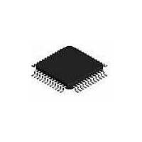
L6740L STMicroelectronics, L6740L Datasheet - Page 41

L6740L
Manufacturer Part Number
L6740L
Description
IC HYBRID CONTROLLERS 48TQFP
Manufacturer
STMicroelectronics
Datasheet
1.L6740LTR.pdf
(44 pages)
Specifications of L6740L
Applications
Hybrid Controllers
Voltage - Supply
9 V ~ 15 V
Current - Supply
20mA
Operating Temperature
0°C ~ 125°C
Mounting Type
Surface Mount
Package / Case
48-TQFP Exposed Pad, 48-eTQFP, 48-HTQFP, 48-VQFP
Number Of Outputs
2
Output Current
170 A
Input Voltage
13.2 V
Mounting Style
SMD/SMT
Maximum Operating Temperature
+ 125 C
Minimum Operating Temperature
0 C
Hybrid Controller
compatible with PVI and SVI CPUs
Dual Controller
2 to 4 scalable phases for CPU CORE, 1 phase for NB
Dual Over-current Protection
Average and per-phase
Lead Free Status / RoHS Status
Lead free / RoHS Compliant
Voltage - Input
-
Lead Free Status / Rohs Status
Lead free / RoHS Compliant
Available stocks
Company
Part Number
Manufacturer
Quantity
Price
Part Number:
L6740L
Manufacturer:
ST
Quantity:
20 000
Part Number:
L6740LTR
Manufacturer:
ST
Quantity:
20 000
L6740L
11
11.1
11.2
Layout guidelines
Layout is one of the most important things to consider when designing high current
applications. A good layout solution can generate a benefit in lowering power dissipation on
the power paths, reducing radiation and a proper connection between signal and power
ground can optimize the performance of the control loops.
Two kind of critical components and connections have to be considered when laying-out a
VRM based on L6740L: power components and connections and small signal components
connections.
Power components and connections
These are the components and connections where switching and high continuous current
flows from the input to the load. The first priority when placing components has to be
reserved to this power section, minimizing the length of each connection and loop as much
as possible. To minimize noise and voltage spikes (EMI and losses) these interconnections
must be a part of a power plane and anyway realized by wide and thick copper traces: loop
must be anyway minimized. The critical components, i.e. the power transistors, must be
close one to the other. The use of multi-layer printed circuit board is recommended.
Since L6740L uses external drivers to switch the power MOSFETs, check the selected
driver documentation for informations related to proper layout for this part.
Small signal components and connections
These are small signal components and connections to critical nodes of the application as
well as bypass capacitors for the device supply. Locate the bypass capacitor close to the
device and refer sensible components such as frequency set-up resistor R
resistor (both sections) and OVP resistor R
connect SGND to PGND plane in a single point to avoid that drops due to the high current
delivered causes errors in the device behavior.
VSEN pin filtered vs. SGND helps in reducing noise injection into device and EN pin filtered
vs. SGND helps in reducing false trip due to coupled noise: take care in routing driving net
for this pin in order to minimize coupled noise.
Remote Buffer Connection must be routed as parallel nets from the FBG/FBR pins to the
load in order to avoid the pick-up of any common mode noise. Connecting these pins in
points far from the load will cause a non-optimum load regulation, increasing output
tolerance.
Locate current reading components close to the device. The PCB traces connecting the
reading point must use dedicated nets, routed as parallel traces in order to avoid the pick-up
of any common mode noise. It's also important to avoid any offset in the measurement and,
to get a better precision, to connect the traces as close as possible to the sensing elements.
Symmetrical layout is also suggested. Small filtering capacitor can be added, near the
controller, between V
higher layout flexibility.
OUT
and SGND, on the CSx- line when reading across inductor to allow
OVP
to SGND. Star grounding is suggested:
Layout guidelines
OSC
, offset
41/44


