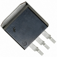
RC1585M Fairchild Semiconductor, RC1585M Datasheet - Page 7

RC1585M
Manufacturer Part Number
RC1585M
Description
IC REG LDO ADJ 5A TO-263
Manufacturer
Fairchild Semiconductor
Datasheet
1.RC1585M15.pdf
(12 pages)
Specifications of RC1585M
Applications
Converter, Pentium® II GTL+, Pro
Voltage - Input
3.5 ~ 7 V
Number Of Outputs
1
Voltage - Output
1.5 ~ 3.6 V
Operating Temperature
0°C ~ 125°C
Mounting Type
Surface Mount
Package / Case
D²Pak, TO-263 (3 leads + tab)
Lead Free Status / RoHS Status
Contains lead / RoHS non-compliant
Available stocks
Company
Part Number
Manufacturer
Quantity
Price
Part Number:
RC1585M
Manufacturer:
FAIRCHILD/仙童
Quantity:
20 000
Part Number:
RC1585M15
Manufacturer:
FAIRCHILD/仙童
Quantity:
20 000
Part Number:
RC1585MC
Manufacturer:
FAIRCHILD/仙童
Quantity:
20 000
Company:
Part Number:
RC1585MT
Manufacturer:
FAIRCHILD
Quantity:
1 250
Part Number:
RC1585MT
Manufacturer:
FAIRCHILD/仙童
Quantity:
20 000
V
Load Regulation
It is not possible to provide true remote load sensing
because the RC1585 series are three-terminal devices.
Load regulation is limited by the resistance of the wire
connecting the regulators to the load. Load regulation
per the data sheet specification is measured at the
bottom of the package.
For fixed voltage devices, negative side sensing is a true
Kelvin connection with the ground pin of the device
returned to the negative side of the load. This is
illustrated in Figure 12.
IN
For adjustable voltage devices, negative side sensing is
a true Kelvin connection with the bottom of the output
divider returned to the negative side of the load. The
best load regulation is obtained when the top of the
resistor divider R1 connects directly to the regulator
output and not to the load. Figure 13 illustrates this
point.
If R1 connects to the load, then the effective resistance
between the regulator and the load would be:
R
Figure 12. Connection for Best Load Regulation
PRODUCT SPECIFICATION
V
7
V
The current out of the adjust pin adds to the current
from R1 and is typically 35 A. Its output voltage
contribution is small and only needs consideration
when a very precise output voltage setting is
required.
P
IN
OUT
C1
10 F
(1 + R2/R1), R
= V
+
IN
Figure 11. Basic Regulator Circuit
RC1585 -1.5
REF
GND
(1 + R2/R1) + I
I
35 A
ADJ
OUT
IN
P
= Parasitic Line Resistance
RC1585
ADJ
OUT
ADJ
(R2)
Line Resistance
V
REF
Parasitic
R
P
R1
R2
R
+
L
C2
22 F
V
Figure 13. Connection for Best Load Regulation
Thermal Considerations
The RC1585 series protect themselves under overload
conditions with internal power and thermal limiting
circuitry. However, for normal continuous load
conditions, do not exceed maximum junction
temperature ratings. It is important to consider all
sources of thermal resistance from junction-to-
ambient. These sources include the junction-to-case
resistance, the case-to-heat sink interface resistance,
and the heat sink resistance. Thermal resistance
specifications have been developed to more accurately
reflect device temperature and ensure safe operating
temperatures. The electrical characteristics section
provides a separate thermal resistance and maximum
junction temperature for both the control circuitry and
the power transistor. Calculate the maximum junction
temperature for both sections to ensure that both
thermal limits are met.
For example, look at using an RC1585T to generate
5A @ 1.5V
OUT
V
multiply R
is about four milliohms per foot with 16-gauge wire.
This translates to 4mV per foot at 1A load current.
At higher load currents, this drop represents a
significant percentage of the overall regulation. It is
important to keep the positive lead between the
regulator and the load as short as possible and to use
large wire or PC board traces.
IN
The connection shown in Figure 13 does not
*Connect R1 to case
IN
Connect R2 to load
RC1585
P
2% from a 3.3V source (3.2V to 3.6V).
ADJ
by the divider ratio. As an example, R
OUT
Line Resistance
R1*
RC1585
R2*
Parasitic
R
P
R
L
P


