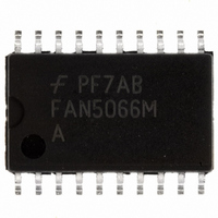
FAN5066MX Fairchild Semiconductor, FAN5066MX Datasheet

FAN5066MX
Specifications of FAN5066MX
FAN5066MX_NL
FAN5066MX_NLTR
FAN5066MX_NLTR
Related parts for FAN5066MX
FAN5066MX Summary of contents
Page 1
... VID2 VID4 VID1 VID3 PRELIMINARY INFORMATION describes products that are not in full production at the time of printing. Specifications are based on design goals and limited characterization. They may change without notice. Contact Fairchild Semiconductor for current information. Description FAN5066 – + – + – ...
Page 2
FAN5066 Pin Assignments Pin Definitions Pin Number Pin Name Pin Function Description 1 CEXT Oscillator Capacitor Connection . Connecting an external capacitor to this pin sets the internal oscillator frequency. Layout of this pin is critical to system performance. See ...
Page 3
PRODUCT SPECIFICATION Absolute Maximum Ratings Supply Voltages, VCCA, VCCP, VCCQP to GND Supply Voltage VCCQP, Charge Pump (V Voltage Identification Code Inputs, VID3-VID0 VREF Output Current Junction Temperature Storage Temperature Lead Soldering Temperature, 10 seconds Operating Conditions Parameter ...
Page 4
FAN5066 Table 1. DAC Output Voltage Programming Codes VID4 VID3 ...
Page 5
PRODUCT SPECIFICATION Typical Operating Characteristics (VCCA, VCCD = 5V 280 KHz, and T OSC Efficiency vs. Output Current 0.1 0.3 0.6 0.9 1.2 1.5 Output Current (A) Output Voltage vs. Output ...
Page 6
FAN5066 Typical Operating Characteristics Output Ripple, 900m @ 3A Time (1 s/division) Switching Waveforms, 3A Load Time (1 s/division) 6 (continued) Transient Response 0.1A Transient Response, 0. Time (1 s/division) Output Startup, System Power-up HIDRV pin ...
Page 7
PRODUCT SPECIFICATION Application Circuit +12V L1 +5V 2 0.1 F 330 F + 324 U2 FAN4041 R7 C9 909 0.1 F VID4 VID3 VID2 VID1 REV. 2.1.4 11/13/01 0 ...
Page 8
FAN5066 Table 2. FAN5066 Application Bill of Materials for 900mV @ 3A Reference Manufacturer Part # C1–3, C6–C9 Panasonic ECU-V1H104ZFX C4–5 Panasonic ECU-V1C105ZFX C Panasonic ext ECU-V1H101JCG C IN AVX TPSE337*010R0100 C OUT AVX TPSE477*006R0100 D1 Motorola 1N4735A L1 Coiltronics ...
Page 9
PRODUCT SPECIFICATION Application Circuit +12V L1 +5V 1 C11 0.1 F 680 F VDDQ R5 499 R6 499 REV. 2.1.4 11/13/ 1N4735A ...
Page 10
FAN5066 Table 3. FAN5066 Application Bill of Materials for DDR VTT Reference Manufacturer Part # C1–2, C6–C9 Panasonic ECU-V1H104ZFX C4–5 Panasonic ECU-V1C105ZFX C10 Panasonic ECU-V1H101JCG C11 Sanyo 6SP680M C OUT Sanyo 4SP820M D1 Motorola 1N4735A L1 Coiltronics UP1B-1R5 L2 Coiltronics ...
Page 11
PRODUCT SPECIFICATION Application Information The FAN5066 Controller Main Control Loop High Current Output Drivers REV. 2.1.4 11/13/01 Power Good (PWRGD) Output Enable (ENABLE) Over-Voltage Protection Over-Current Protection Oscillator FAN5066 11 ...
Page 12
FAN5066 Design Considerations and Component Selection MOSFET Selection MOSFET Gate Bias Method 1. Charge Pump (Bootstrap) 12 PRODUCT SPECIFICATION D1 VCCQP HIDRV CP PWM/PFM Control LODRV GNDP Figure 4. Charge Pump Configuration Method 2. 12V Gate Bias +12V 47 D1 ...
Page 13
PRODUCT SPECIFICATION Inductor Selection ESR in out out L min ripple out max FAN5066 Short Circuit Current Characteristics REV. 2.1.4 ...
Page 14
FAN5066 Input Filter 2 0.1 F Figure 7. Input Filter Droop Resistor SENSE DROOP Q2 IFB VFB Figure 8. Use of a Droop Resistor 14 PCB Layout Guidelines Vin 1000 F, 10V Electrolytic VO ...
Page 15
PRODUCT SPECIFICATION Additional Information REV. 2.1.4 11/13/01 FAN5066 15 ...
Page 16
FAN5066 Mechanical Dimensions – 20 Lead SOIC Inches Millimeters Symbol Min. Max. Min. A .093 .104 2.35 A1 .004 .012 0.10 B .013 .020 0.33 C .009 .013 0.23 D .496 .512 12.60 E .291 .299 7.40 e .050 BSC ...
Page 17
PRODUCT SPECIFICATION Mechanical Dimensions – 20 Lead TSSOP Inches Millimeters Symbol Min. Max. Min. A — .047 — A1 .002 .006 0.05 B .007 0.19 .012 C .004 .008 0.09 D .252 .260 6.40 E .169 .177 4.30 e .026 ...
Page 18
... FAN5066MTCX 20 pin TSSOP DISCLAIMER FAIRCHILD SEMICONDUCTOR RESERVES THE RIGHT TO MAKE CHANGES WITHOUT FURTHER NOTICE TO ANY PRODUCTS HEREIN TO IMPROVE RELIABILITY, FUNCTION OR DESIGN. FAIRCHILD DOES NOT ASSUME ANY LIABILITY ARISING OUT OF THE APPLICATION OR USE OF ANY PRODUCT OR CIRCUIT DESCRIBED HEREIN; NEITHER DOES IT CONVEY ANY LICENSE UNDER ITS PATENT RIGHTS, NOR THE RIGHTS OF OTHERS. ...


