PCM18XT0 Microchip Technology, PCM18XT0 Datasheet - Page 259
PCM18XT0
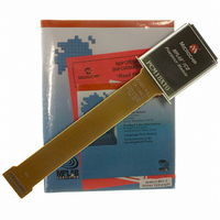
Manufacturer Part Number
PCM18XT0
Description
MODULE PROC PIC18F4685
Manufacturer
Microchip Technology
Datasheet
1.PCM18XT0.pdf
(484 pages)
Specifications of PCM18XT0
Accessory Type
Processor Module
Product
Microcontroller Modules
Core Processor
PIC18F4685
Lead Free Status / RoHS Status
Not applicable / Not applicable
For Use With/related Products
ICE2000
For Use With
ICE2000 - EMULATOR MPLAB-ICE 2000 POD
Lead Free Status / RoHS Status
Lead free / RoHS Compliant, Not applicable / Not applicable


20.0
The analog comparator module contains two compara-
tors that can be configured in a variety of ways. The
inputs can be selected from the analog inputs multiplexed
with pins RA0 through RA5, as well as the on-chip volt-
age reference (see Section 21.0 “Comparator Voltage
Reference Module”). The digital outputs (normal or
inverted) are available at the pin level and can also be
read through the control register.
REGISTER 20-1:
© 2009 Microchip Technology Inc.
bit 7
Legend:
R = Readable bit
-n = Value at POR
bit 7
bit 6
bit 5
bit 4
bit 3
bit 2-0
Note:
C2OUT
R-0
COMPARATOR MODULE
Comparators are only available in 40/44-pin
devices (PIC18F4682/4685).
C2OUT: Comparator 2 Output bit
When C2INV = 0:
1 = C2 V
0 = C2 V
When C2INV = 1:
1 = C2 V
0 = C2 V
C1OUT: Comparator 1 Output bit
When C1INV = 0:
1 = C1 V
0 = C1 V
When C1INV = 1:
1 = C1 V
0 = C1 V
C2INV: Comparator 2 Output Inversion bit
1 = C2 output inverted
0 = C2 output not inverted
C1INV: Comparator 1 Output Inversion bit
1 = C1 output inverted
0 = C1 output not inverted
CIS: Comparator Input Switch bit
When CM2:CM0 = 110:
1 = C1 V
0 = C1 V
CM2:CM0: Comparator Mode bits
Figure 20-1 shows the Comparator modes and the CM2:CM0 bit settings.
C1OUT
C2 V
C2 V
R-0
CMCON: COMPARATOR CONTROL REGISTER
IN
IN
IN
IN
IN
IN
IN
IN
IN
IN
IN
IN
+ > C2 V
+ < C2 V
+ < C2 V
+ > C2 V
+ > C1 V
+ < C1 V
+ < C1 V
+ > C1 V
- connects to RD0/PSP0/C1IN+
- connects to RD2/PSP2/C2IN+
- connects to RD1/PSP1/C1IN-
- connects to RD3/PSP3/C2IN-
W = Writable bit
‘1’ = Bit is set
C2INV
R/W-0
IN
IN
IN
IN
IN
IN
IN
IN
-
-
-
-
-
-
-
-
PIC18F2682/2685/4682/4685
C1INV
R/W-0
U = Unimplemented bit, read as ‘0’
‘0’ = Bit is cleared
R/W-0
The CMCON register (Register 20-1) selects the
comparator input and output configuration. Block
diagrams of the various comparator configurations are
shown in Figure 20-1.
CIS
R/W-0
CM2
x = Bit is unknown
R/W-0
CM1
DS39761C-page 259
R/W-0
CM0
bit 0
Related parts for PCM18XT0
Image
Part Number
Description
Manufacturer
Datasheet
Request
R

Part Number:
Description:
Manufacturer:
Microchip Technology Inc.
Datasheet:
Part Number:
Description:
Manufacturer:
Microchip Technology Inc.
Datasheet:
Part Number:
Description:
Manufacturer:
Microchip Technology Inc.
Datasheet:
Part Number:
Description:
Manufacturer:
Microchip Technology Inc.
Datasheet:
Part Number:
Description:
Manufacturer:
Microchip Technology Inc.
Datasheet:
Part Number:
Description:
Manufacturer:
Microchip Technology Inc.
Datasheet:
Part Number:
Description:
Manufacturer:
Microchip Technology Inc.
Datasheet:
Part Number:
Description:
Manufacturer:
Microchip Technology Inc.
Datasheet: