PCM18XT0 Microchip Technology, PCM18XT0 Datasheet - Page 99
PCM18XT0
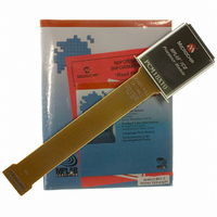
Manufacturer Part Number
PCM18XT0
Description
MODULE PROC PIC18F4685
Manufacturer
Microchip Technology
Datasheet
1.PCM18XT0.pdf
(484 pages)
Specifications of PCM18XT0
Accessory Type
Processor Module
Product
Microcontroller Modules
Core Processor
PIC18F4685
Lead Free Status / RoHS Status
Not applicable / Not applicable
For Use With/related Products
ICE2000
For Use With
ICE2000 - EMULATOR MPLAB-ICE 2000 POD
Lead Free Status / RoHS Status
Lead free / RoHS Compliant, Not applicable / Not applicable


REGISTER 6-1:
© 2009 Microchip Technology Inc.
bit 7
Legend:
R = Readable bit
-n = Value at POR
bit 7
bit 6
bit 5
bit 4
bit 3
bit 2
bit 1
bit 0
Note 1:
EEPGD
R/W-x
When a WRERR occurs, the EEPGD and CFGS bits are not cleared. This allows tracing of the error
condition.
EEPGD: Flash Program or Data EEPROM Memory Select bit
1 = Access Flash program memory
0 = Access data EEPROM memory
CFGS: Flash Program/Data EEPROM or Configuration Select bit
1 = Access Configuration registers
0 = Access Flash program or data EEPROM memory
Unimplemented: Read as ‘0’
FREE: Flash Row Erase Enable bit
1 = Erase the program memory row addressed by TBLPTR on the next WR command (cleared by
0 = Perform write-only
WRERR: Flash Program/Data EEPROM Error Flag bit
1 = A write operation is prematurely terminated (any Reset during self-timed programming in normal
0 = The write operation completed
WREN: Flash Program/Data EEPROM Write Enable bit
1 = Allows write cycles to Flash program/data EEPROM
0 = Inhibits write cycles to Flash program/data EEPROM
WR: Write Control bit
1 = Initiates a data EEPROM erase/write cycle or a program memory erase cycle or write cycle
0 = Write cycle to the EEPROM is complete
RD: Read Control bit
1 = Initiates an EEPROM read (Read takes one cycle. RD is cleared in hardware. The RD bit can only
0 = Does not initiate an EEPROM read
CFGS
R/W-x
completion of erase operation)
operation or an improper write attempt)
(The operation is self-timed and the bit is cleared by hardware once write is complete.
The WR bit can only be set (not cleared) in software.)
be set (not cleared) in software. RD bit cannot be set when EEPGD = 1 or CFGS = 1.)
EECON1: DATA EEPROM CONTROL REGISTER 1
S = Settable bit
W = Writable bit
‘1’ = Bit is set
U-0
—
PIC18F2682/2685/4682/4685
R/W-0
FREE
U = Unimplemented bit, read as ‘0’
‘0’ = Bit is cleared
WRERR
R/W-x
(1)
(1)
WREN
R/W-0
x = Bit is unknown
R/S-0
WR
DS39761C-page 99
R/S-0
RD
bit 0
Related parts for PCM18XT0
Image
Part Number
Description
Manufacturer
Datasheet
Request
R

Part Number:
Description:
Manufacturer:
Microchip Technology Inc.
Datasheet:
Part Number:
Description:
Manufacturer:
Microchip Technology Inc.
Datasheet:
Part Number:
Description:
Manufacturer:
Microchip Technology Inc.
Datasheet:
Part Number:
Description:
Manufacturer:
Microchip Technology Inc.
Datasheet:
Part Number:
Description:
Manufacturer:
Microchip Technology Inc.
Datasheet:
Part Number:
Description:
Manufacturer:
Microchip Technology Inc.
Datasheet:
Part Number:
Description:
Manufacturer:
Microchip Technology Inc.
Datasheet:
Part Number:
Description:
Manufacturer:
Microchip Technology Inc.
Datasheet: