DTMFDECODER-RD Silicon Laboratories Inc, DTMFDECODER-RD Datasheet - Page 173
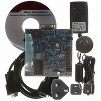
DTMFDECODER-RD
Manufacturer Part Number
DTMFDECODER-RD
Description
KIT REF DESIGN DTMF DECODER
Manufacturer
Silicon Laboratories Inc
Specifications of DTMFDECODER-RD
Mfg Application Notes
DTMF Decoder Ref Design AppNote
Main Purpose
Telecom, DTMF Decoder
Embedded
No
Utilized Ic / Part
C8051F300
Primary Attributes
8kHz Sampling Rate ADC
Secondary Attributes
16 Goertzel Filters
Processor To Be Evaluated
C8051F300
Interface Type
RS-232
Lead Free Status / RoHS Status
Contains lead / RoHS non-compliant
Lead Free Status / RoHS Status
Lead free / RoHS Compliant, Contains lead / RoHS non-compliant
Other names
336-1283


17. C2 Interface
C8051F300/1/2/3/4/5 devices include an on-chip Silicon Labs 2-Wire (C2) debug interface to allow Flash
programming and in-system debugging with the production part installed in the end application. The C2
interface operates using only two pins: a bi-directional data signal (C2D) and a clock input (C2CK). See the
C2 Interface Specification for details on the C2 protocol.
17.1. C2 Interface Registers
The following describes the C2 registers necessary to perform Flash programming functions through the
C2 interface. All C2 registers are accessed through the C2 interface as described in the C2 Interface Spec-
ification.
Bits7–0: The C2ADD register is accessed via the C2 interface to select the target Data register for
This read-only register returns the 8-bit device ID: 0x04 (C8051F300/1/2/3/4/5).
Bit7
Bit7
C2 Data Read and Data Write commands.
Address
0xB4
0xF1
0xA4
0x00
0x01
0x02
0x80
Bit6
Bit6
C2 Register Definition 17.2.
C2 Register Definition 17.1.
Bit5
Bit5
Selects the Device ID register for Data Read instructions
Selects the Revision ID register for Data Read instructions
Selects the C2 Flash Programming Control register for Data
Read/Write instructions
Selects the C2 Flash Programming Data register for Data
Read/Write instructions
Selects the Port0 register for Data Read/Write instructions
Selects the Port0 Input Mode register for Data Read/Write instruc-
tions
Selects the Port0 Output Mode register for Data Read/Write
instructions
Bit4
Bit4
Rev. 2.9
Bit3
Bit3
DEVICEID: C2 Device ID
Description
C2ADD: C2 Address
Bit2
Bit2
C8051F300/1/2/3/4/5
Bit1
Bit1
Bit0
Bit0
00000000
00000100
Reset Value
Reset Value
173
Related parts for DTMFDECODER-RD
Image
Part Number
Description
Manufacturer
Datasheet
Request
R

Part Number:
Description:
SMD/C°/SINGLE-ENDED OUTPUT SILICON OSCILLATOR
Manufacturer:
Silicon Laboratories Inc
Part Number:
Description:
Manufacturer:
Silicon Laboratories Inc
Datasheet:
Part Number:
Description:
N/A N/A/SI4010 AES KEYFOB DEMO WITH LCD RX
Manufacturer:
Silicon Laboratories Inc
Datasheet:
Part Number:
Description:
N/A N/A/SI4010 SIMPLIFIED KEY FOB DEMO WITH LED RX
Manufacturer:
Silicon Laboratories Inc
Datasheet:
Part Number:
Description:
N/A/-40 TO 85 OC/EZLINK MODULE; F930/4432 HIGH BAND (REV E/B1)
Manufacturer:
Silicon Laboratories Inc
Part Number:
Description:
EZLink Module; F930/4432 Low Band (rev e/B1)
Manufacturer:
Silicon Laboratories Inc
Part Number:
Description:
I°/4460 10 DBM RADIO TEST CARD 434 MHZ
Manufacturer:
Silicon Laboratories Inc
Part Number:
Description:
I°/4461 14 DBM RADIO TEST CARD 868 MHZ
Manufacturer:
Silicon Laboratories Inc
Part Number:
Description:
I°/4463 20 DBM RFSWITCH RADIO TEST CARD 460 MHZ
Manufacturer:
Silicon Laboratories Inc
Part Number:
Description:
I°/4463 20 DBM RADIO TEST CARD 868 MHZ
Manufacturer:
Silicon Laboratories Inc
Part Number:
Description:
I°/4463 27 DBM RADIO TEST CARD 868 MHZ
Manufacturer:
Silicon Laboratories Inc
Part Number:
Description:
I°/4463 SKYWORKS 30 DBM RADIO TEST CARD 915 MHZ
Manufacturer:
Silicon Laboratories Inc
Part Number:
Description:
N/A N/A/-40 TO 85 OC/4463 RFMD 30 DBM RADIO TEST CARD 915 MHZ
Manufacturer:
Silicon Laboratories Inc
Part Number:
Description:
I°/4463 20 DBM RADIO TEST CARD 169 MHZ
Manufacturer:
Silicon Laboratories Inc