DTMFDECODER-RD Silicon Laboratories Inc, DTMFDECODER-RD Datasheet - Page 39
DTMFDECODER-RD
Manufacturer Part Number
DTMFDECODER-RD
Description
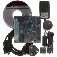
KIT REF DESIGN DTMF DECODER
Manufacturer
Silicon Laboratories Inc
Specifications of DTMFDECODER-RD
Mfg Application Notes
DTMF Decoder Ref Design AppNote
Main Purpose
Telecom, DTMF Decoder
Embedded
No
Utilized Ic / Part
C8051F300
Primary Attributes
8kHz Sampling Rate ADC
Secondary Attributes
16 Goertzel Filters
Processor To Be Evaluated
C8051F300
Interface Type
RS-232
Lead Free Status / RoHS Status
Contains lead / RoHS non-compliant
Lead Free Status / RoHS Status
Lead free / RoHS Compliant, Contains lead / RoHS non-compliant
Other names
336-1283


5.3.
ADC0 has a maximum conversion speed of 500 ksps. The ADC0 conversion clock is a divided version of
the system clock, determined by the AD0SC bits in the ADC0CF register (system clock divided by
(AD0SC + 1) for 0 AD0SC 31).
5.3.1. Starting a Conversion
A conversion can be initiated in one of five ways, depending on the programmed states of the ADC0 Start
of Conversion Mode bits (AD0CM2–0) in register ADC0CN. Conversions may be initiated by one of the fol-
lowing:
Writing a ‘1’ to AD0BUSY provides software control of ADC0 whereby conversions are performed "on-
demand". During conversion, the AD0BUSY bit is set to logic 1 and reset to logic 0 when the conversion is
complete. The falling edge of AD0BUSY triggers an interrupt (when enabled) and sets the ADC0 interrupt
flag (AD0INT). Note: When polling for ADC conversion completions, the ADC0 interrupt flag (AD0INT)
should be used. Converted data is available in the ADC0 data register, ADC0, when bit AD0INT is logic 1.
Note that when Timer 2 overflows are used as the conversion source, Timer 2 Low Byte overflows are
used if Timer 2 is in 8-bit mode; Timer 2 High byte overflows are used if Timer 2 is in 16-bit mode. See
tion “15. Timers” on page 143
Important Note About Using CNVSTR: The CNVSTR input pin also functions as Port pin P0.6. When the
CNVSTR input is used as the ADC0 conversion source, Port pin P0.6 should be skipped by the Digital
Crossbar. To configure the Crossbar to skip P0.6, set to ‘1’ Bit6 in register XBR0. See
Input/Output” on page 103
Modes of Operation
1. Writing a ‘1’ to the AD0BUSY bit of register ADC0CN
2. A Timer 0 overflow (i.e. timed continuous conversions)
3. A Timer 2 overflow
4. A Timer 1 overflow
5. A rising edge on the CNVSTR input signal (pin P0.6)
for details on Port I/O configuration.
for timer configuration.
Rev. 2.9
C8051F300/1/2/3/4/5
Section “12. Port
Sec-
39
Related parts for DTMFDECODER-RD
Image
Part Number
Description
Manufacturer
Datasheet
Request
R

Part Number:
Description:
SMD/C°/SINGLE-ENDED OUTPUT SILICON OSCILLATOR
Manufacturer:
Silicon Laboratories Inc
Part Number:
Description:
Manufacturer:
Silicon Laboratories Inc
Datasheet:
Part Number:
Description:
N/A N/A/SI4010 AES KEYFOB DEMO WITH LCD RX
Manufacturer:
Silicon Laboratories Inc
Datasheet:
Part Number:
Description:
N/A N/A/SI4010 SIMPLIFIED KEY FOB DEMO WITH LED RX
Manufacturer:
Silicon Laboratories Inc
Datasheet:
Part Number:
Description:
N/A/-40 TO 85 OC/EZLINK MODULE; F930/4432 HIGH BAND (REV E/B1)
Manufacturer:
Silicon Laboratories Inc
Part Number:
Description:
EZLink Module; F930/4432 Low Band (rev e/B1)
Manufacturer:
Silicon Laboratories Inc
Part Number:
Description:
I°/4460 10 DBM RADIO TEST CARD 434 MHZ
Manufacturer:
Silicon Laboratories Inc
Part Number:
Description:
I°/4461 14 DBM RADIO TEST CARD 868 MHZ
Manufacturer:
Silicon Laboratories Inc
Part Number:
Description:
I°/4463 20 DBM RFSWITCH RADIO TEST CARD 460 MHZ
Manufacturer:
Silicon Laboratories Inc
Part Number:
Description:
I°/4463 20 DBM RADIO TEST CARD 868 MHZ
Manufacturer:
Silicon Laboratories Inc
Part Number:
Description:
I°/4463 27 DBM RADIO TEST CARD 868 MHZ
Manufacturer:
Silicon Laboratories Inc
Part Number:
Description:
I°/4463 SKYWORKS 30 DBM RADIO TEST CARD 915 MHZ
Manufacturer:
Silicon Laboratories Inc
Part Number:
Description:
N/A N/A/-40 TO 85 OC/4463 RFMD 30 DBM RADIO TEST CARD 915 MHZ
Manufacturer:
Silicon Laboratories Inc
Part Number:
Description:
I°/4463 20 DBM RADIO TEST CARD 169 MHZ
Manufacturer:
Silicon Laboratories Inc