DTMFDECODER-RD Silicon Laboratories Inc, DTMFDECODER-RD Datasheet - Page 26
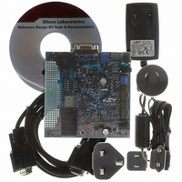
DTMFDECODER-RD
Manufacturer Part Number
DTMFDECODER-RD
Description
KIT REF DESIGN DTMF DECODER
Manufacturer
Silicon Laboratories Inc
Specifications of DTMFDECODER-RD
Mfg Application Notes
DTMF Decoder Ref Design AppNote
Main Purpose
Telecom, DTMF Decoder
Embedded
No
Utilized Ic / Part
C8051F300
Primary Attributes
8kHz Sampling Rate ADC
Secondary Attributes
16 Goertzel Filters
Processor To Be Evaluated
C8051F300
Interface Type
RS-232
Lead Free Status / RoHS Status
Contains lead / RoHS non-compliant
Lead Free Status / RoHS Status
Lead free / RoHS Compliant, Contains lead / RoHS non-compliant
Other names
336-1283


C8051F300/1/2/3/4/5
Table 3.1. Global Electrical Characteristics (Continued)
–40 to +85 °C, 25 MHz system clock unless otherwise specified.
26
I
I
(Note 3, Note 5)
Digital Supply Current
(Stop Mode, shutdown)
Notes:
DD
DD
1. Given in Table 9.2 on page 86.
2. SYSCLK must be at least 32 kHz to enable debugging.
3. Based on device characterization data; Not production tested.
4. Normal IDD can be estimated for frequencies <= 15 MHz by simply multiplying the frequency of interest by
5. Idle IDD can be estimated for frequencies <= 1 MHz by simply multiplying the frequency of interest by the
Supply Sensitivity (Note 3) F = 25 MHz
Frequency Sensitivity
the frequency sensitivity number for that range. When using these numbers to estimate I
estimate should be the current at 25 MHz minus the difference in current indicated by the frequency sensitivity
number.
For example: V
frequency sensitivity number for that range. When using these numbers to estimate Idle I
estimate should be the current at 25 MHz minus the difference in current indicated by the frequency sensitivity
number.
For example: V
Parameter
DD
DD
= 3.0 V; F = 20 MHz, I
= 3.0 V; F = 5 MHz, Idle I
F = 1 MHz
V
V
V
V
Oscillator not running,
V
DD
DD
DD
DD
DD
= 3.0 V, F <= 1 MHz, T = 25
= 3.0 V, F > 1 MHz, T = 25
= 3.6 V, F <= 1 MHz, T = 25
= 3.6 V, F > 1 MHz, T = 25
Monitor Disabled
DD
Conditions
DD
= 6.6 mA – (25 MHz – 20 MHz) x 0.16 mA/MHz = 5.8 mA.
Rev. 2.9
= 3.3 mA – (25 MHz – 5 MHz) x 0.10 mA/MHz = 1.3 mA.
°
°
C
C
°
°
C
C
Min
—
—
—
—
—
—
—
< 0.1
0.27
0.10
0.35
0.12
Typ
47
59
DD
DD
Max
for >15 MHz, the
for >1 MHz, the
—
—
—
—
—
—
—
mA/MHz
mA/MHz
mA/MHz
mA/MHz
Units
%/V
%/V
µA
Related parts for DTMFDECODER-RD
Image
Part Number
Description
Manufacturer
Datasheet
Request
R

Part Number:
Description:
SMD/C°/SINGLE-ENDED OUTPUT SILICON OSCILLATOR
Manufacturer:
Silicon Laboratories Inc
Part Number:
Description:
Manufacturer:
Silicon Laboratories Inc
Datasheet:
Part Number:
Description:
N/A N/A/SI4010 AES KEYFOB DEMO WITH LCD RX
Manufacturer:
Silicon Laboratories Inc
Datasheet:
Part Number:
Description:
N/A N/A/SI4010 SIMPLIFIED KEY FOB DEMO WITH LED RX
Manufacturer:
Silicon Laboratories Inc
Datasheet:
Part Number:
Description:
N/A/-40 TO 85 OC/EZLINK MODULE; F930/4432 HIGH BAND (REV E/B1)
Manufacturer:
Silicon Laboratories Inc
Part Number:
Description:
EZLink Module; F930/4432 Low Band (rev e/B1)
Manufacturer:
Silicon Laboratories Inc
Part Number:
Description:
I°/4460 10 DBM RADIO TEST CARD 434 MHZ
Manufacturer:
Silicon Laboratories Inc
Part Number:
Description:
I°/4461 14 DBM RADIO TEST CARD 868 MHZ
Manufacturer:
Silicon Laboratories Inc
Part Number:
Description:
I°/4463 20 DBM RFSWITCH RADIO TEST CARD 460 MHZ
Manufacturer:
Silicon Laboratories Inc
Part Number:
Description:
I°/4463 20 DBM RADIO TEST CARD 868 MHZ
Manufacturer:
Silicon Laboratories Inc
Part Number:
Description:
I°/4463 27 DBM RADIO TEST CARD 868 MHZ
Manufacturer:
Silicon Laboratories Inc
Part Number:
Description:
I°/4463 SKYWORKS 30 DBM RADIO TEST CARD 915 MHZ
Manufacturer:
Silicon Laboratories Inc
Part Number:
Description:
N/A N/A/-40 TO 85 OC/4463 RFMD 30 DBM RADIO TEST CARD 915 MHZ
Manufacturer:
Silicon Laboratories Inc
Part Number:
Description:
I°/4463 20 DBM RADIO TEST CARD 169 MHZ
Manufacturer:
Silicon Laboratories Inc