DTMFDECODER-RD Silicon Laboratories Inc, DTMFDECODER-RD Datasheet - Page 70
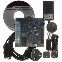
DTMFDECODER-RD
Manufacturer Part Number
DTMFDECODER-RD
Description
KIT REF DESIGN DTMF DECODER
Manufacturer
Silicon Laboratories Inc
Specifications of DTMFDECODER-RD
Mfg Application Notes
DTMF Decoder Ref Design AppNote
Main Purpose
Telecom, DTMF Decoder
Embedded
No
Utilized Ic / Part
C8051F300
Primary Attributes
8kHz Sampling Rate ADC
Secondary Attributes
16 Goertzel Filters
Processor To Be Evaluated
C8051F300
Interface Type
RS-232
Lead Free Status / RoHS Status
Contains lead / RoHS non-compliant
Lead Free Status / RoHS Status
Lead free / RoHS Compliant, Contains lead / RoHS non-compliant
Other names
336-1283


C8051F300/1/2/3/4/5
70
Bit7:
Bit6:
Bit5:
Bits4–3: RS1-RS0: Register Bank Select.
Bit2:
Bit1:
Bit0:
R/W
CY
Bit7
CY: Carry Flag.
This bit is set when the last arithmetic operation resulted in a carry (addition) or a borrow
(subtraction). It is cleared to logic 0 by all other arithmetic operations.
AC: Auxiliary Carry Flag
This bit is set when the last arithmetic operation resulted in a carry into (addition) or a borrow
from (subtraction) the high order nibble. It is cleared to logic 0 by all other arithmetic opera-
tions.
F0: User Flag 0.
This is a bit-addressable, general purpose flag for use under software control.
These bits select which register bank is used during register accesses.
OV: Overflow Flag.
This bit is set to 1 under the following circumstances:
F1: User Flag 1.
This is a bit-addressable, general purpose flag for use under software control.
PARITY: Parity Flag.
This bit is set to logic 1 if the sum of the eight bits in the accumulator is odd and cleared if the
sum is even.
• An ADD, ADDC, or SUBB instruction causes a sign-change overflow.
• A MUL instruction results in an overflow (result is greater than 255).
• A DIV instruction causes a divide-by-zero condition.
The OV bit is cleared to 0 by the ADD, ADDC, SUBB, MUL, and DIV instructions in all other
cases.
RS1
R/W
0
0
1
1
AC
Bit6
SFR Definition 8.4.
RS0
0
1
0
1
R/W
Bit5
F0
Register Bank
RS1
R/W
Bit4
0
1
2
3
PSW: Program Status Word
RS0
Rev. 2.9
R/W
Bit3
0x00–0x07
0x08–0x0F
0x10–0x17
0x18–0x1F
Address
R/W
OV
Bit2
R/W
Bit1
F1
(bit addressable)
PARITY 00000000
Bit0
R
SFR Address:
Reset Value
0xD0
Related parts for DTMFDECODER-RD
Image
Part Number
Description
Manufacturer
Datasheet
Request
R

Part Number:
Description:
SMD/C°/SINGLE-ENDED OUTPUT SILICON OSCILLATOR
Manufacturer:
Silicon Laboratories Inc
Part Number:
Description:
Manufacturer:
Silicon Laboratories Inc
Datasheet:
Part Number:
Description:
N/A N/A/SI4010 AES KEYFOB DEMO WITH LCD RX
Manufacturer:
Silicon Laboratories Inc
Datasheet:
Part Number:
Description:
N/A N/A/SI4010 SIMPLIFIED KEY FOB DEMO WITH LED RX
Manufacturer:
Silicon Laboratories Inc
Datasheet:
Part Number:
Description:
N/A/-40 TO 85 OC/EZLINK MODULE; F930/4432 HIGH BAND (REV E/B1)
Manufacturer:
Silicon Laboratories Inc
Part Number:
Description:
EZLink Module; F930/4432 Low Band (rev e/B1)
Manufacturer:
Silicon Laboratories Inc
Part Number:
Description:
I°/4460 10 DBM RADIO TEST CARD 434 MHZ
Manufacturer:
Silicon Laboratories Inc
Part Number:
Description:
I°/4461 14 DBM RADIO TEST CARD 868 MHZ
Manufacturer:
Silicon Laboratories Inc
Part Number:
Description:
I°/4463 20 DBM RFSWITCH RADIO TEST CARD 460 MHZ
Manufacturer:
Silicon Laboratories Inc
Part Number:
Description:
I°/4463 20 DBM RADIO TEST CARD 868 MHZ
Manufacturer:
Silicon Laboratories Inc
Part Number:
Description:
I°/4463 27 DBM RADIO TEST CARD 868 MHZ
Manufacturer:
Silicon Laboratories Inc
Part Number:
Description:
I°/4463 SKYWORKS 30 DBM RADIO TEST CARD 915 MHZ
Manufacturer:
Silicon Laboratories Inc
Part Number:
Description:
N/A N/A/-40 TO 85 OC/4463 RFMD 30 DBM RADIO TEST CARD 915 MHZ
Manufacturer:
Silicon Laboratories Inc
Part Number:
Description:
I°/4463 20 DBM RADIO TEST CARD 169 MHZ
Manufacturer:
Silicon Laboratories Inc