DTMFDECODER-RD Silicon Laboratories Inc, DTMFDECODER-RD Datasheet - Page 49
DTMFDECODER-RD
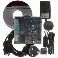
Manufacturer Part Number
DTMFDECODER-RD
Description
KIT REF DESIGN DTMF DECODER
Manufacturer
Silicon Laboratories Inc
Specifications of DTMFDECODER-RD
Mfg Application Notes
DTMF Decoder Ref Design AppNote
Main Purpose
Telecom, DTMF Decoder
Embedded
No
Utilized Ic / Part
C8051F300
Primary Attributes
8kHz Sampling Rate ADC
Secondary Attributes
16 Goertzel Filters
Processor To Be Evaluated
C8051F300
Interface Type
RS-232
Lead Free Status / RoHS Status
Contains lead / RoHS non-compliant
Lead Free Status / RoHS Status
Lead free / RoHS Compliant, Contains lead / RoHS non-compliant
Other names
336-1283


6.
The voltage reference MUX on C8051F300/2 devices is configurable to use an externally connected volt-
age reference or the power supply voltage, V
register (REF0CN) selects the reference source. For an external source, REFSL should be set to ‘0’; For
V
The BIASE bit enables the internal voltage bias generator, which is used by the ADC, Temperature Sensor,
and Internal Oscillator. This bit is forced to logic 1 when any of the aforementioned peripherals is enabled.
The bias generator may be enabled manually by writing a ‘1’ to the BIASE bit in register REF0CN; see
SFR Definition 6.1 for REF0CN register details. The electrical specifications for the voltage reference cir-
cuit are given in Table 6.1.
Important Note About the VREF Input: Port pin P0.0 is used as the external VREF input. When using an
external voltage reference, P0.0 should be configured as analog input and skipped by the Digital Crossbar.
To configure P0.0 as analog input, set to ‘1’ Bit0 in register P0MDIN. To configure the Crossbar to skip
P0.0, set to ‘1’ Bit0 in register XBR0. Refer to
Port I/O configuration details. The external reference voltage must be within the range 0 VREF V
On C8051F300/2 devices, the temperature sensor connects to the highest order input of the ADC0 positive
input multiplexer (see
bit in register REF0CN enables/disables the temperature sensor. While disabled, the temperature sensor
defaults to a high impedance state and any ADC0 measurements performed on the sensor result in mean-
ingless data.
DD
as the reference source, REFSL should be set to ‘1’.
VDD
GND
Voltage Reference (C8051F300/2)
R1
Reference
External
Voltage
Circuit
Figure 6.1. Voltage Reference Functional Block Diagram
Section “5.1. Analog Multiplexer and PGA” on page 36
VREF
VDD
REF0CN
DD
Section “12. Port Input/Output” on page 103
0
1
(see Figure 6.1). The REFSL bit in the Reference Control
Rev. 2.9
IOSCEN
EN
EN
C8051F300/1/2/3/4/5
Bias Generator
Temp Sensor
for details). The TEMPE
To Analog Mux
Internal
VREF
(to ADC)
To ADC, Internal
Oscillator,
Temperature Sensor
for complete
DD
.
49
Related parts for DTMFDECODER-RD
Image
Part Number
Description
Manufacturer
Datasheet
Request
R

Part Number:
Description:
SMD/C°/SINGLE-ENDED OUTPUT SILICON OSCILLATOR
Manufacturer:
Silicon Laboratories Inc
Part Number:
Description:
Manufacturer:
Silicon Laboratories Inc
Datasheet:
Part Number:
Description:
N/A N/A/SI4010 AES KEYFOB DEMO WITH LCD RX
Manufacturer:
Silicon Laboratories Inc
Datasheet:
Part Number:
Description:
N/A N/A/SI4010 SIMPLIFIED KEY FOB DEMO WITH LED RX
Manufacturer:
Silicon Laboratories Inc
Datasheet:
Part Number:
Description:
N/A/-40 TO 85 OC/EZLINK MODULE; F930/4432 HIGH BAND (REV E/B1)
Manufacturer:
Silicon Laboratories Inc
Part Number:
Description:
EZLink Module; F930/4432 Low Band (rev e/B1)
Manufacturer:
Silicon Laboratories Inc
Part Number:
Description:
I°/4460 10 DBM RADIO TEST CARD 434 MHZ
Manufacturer:
Silicon Laboratories Inc
Part Number:
Description:
I°/4461 14 DBM RADIO TEST CARD 868 MHZ
Manufacturer:
Silicon Laboratories Inc
Part Number:
Description:
I°/4463 20 DBM RFSWITCH RADIO TEST CARD 460 MHZ
Manufacturer:
Silicon Laboratories Inc
Part Number:
Description:
I°/4463 20 DBM RADIO TEST CARD 868 MHZ
Manufacturer:
Silicon Laboratories Inc
Part Number:
Description:
I°/4463 27 DBM RADIO TEST CARD 868 MHZ
Manufacturer:
Silicon Laboratories Inc
Part Number:
Description:
I°/4463 SKYWORKS 30 DBM RADIO TEST CARD 915 MHZ
Manufacturer:
Silicon Laboratories Inc
Part Number:
Description:
N/A N/A/-40 TO 85 OC/4463 RFMD 30 DBM RADIO TEST CARD 915 MHZ
Manufacturer:
Silicon Laboratories Inc
Part Number:
Description:
I°/4463 20 DBM RADIO TEST CARD 169 MHZ
Manufacturer:
Silicon Laboratories Inc