DM330023 Microchip Technology, DM330023 Datasheet - Page 36
DM330023
Manufacturer Part Number
DM330023
Description
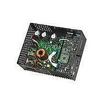
BOARD DEV DSPICDEM MCHV
Manufacturer
Microchip Technology
Series
dsPICDEM™r
Datasheet
1.DM330023.pdf
(64 pages)
Specifications of DM330023
Main Purpose
Power Management, Motor Control
Embedded
Yes, Other
Utilized Ic / Part
dsPIC33F
Primary Attributes
AC Induction (ACIM) Motors, Brushless DC (BLDC) Motors, Permanent Magnet Synchronous (PMSM) Motors
Secondary Attributes
Power Factor Corrected (PFC)
Processor To Be Evaluated
dsPICDEM
Processor Series
dsPIC DSC
Interface Type
RS-232, USB
Operating Supply Voltage
90 V to 265 V
Lead Free Status / RoHS Status
Lead free / RoHS Compliant
Lead Free Status / RoHS Status
Lead free / RoHS Compliant, Lead free / RoHS Compliant
Available stocks
Company
Part Number
Manufacturer
Quantity
Price
Company:

Part Number:
DM330023
Manufacturer:
Microchip Technology
Quantity:
135
Company:
Part Number:
DM330023-2
Manufacturer:
MICROCHIP
Quantity:
12 000


dsPICDEM™ MCHV Development System User’s Guide
DS70605A-page 30
4.1.2
The active PFC circuit is essentially a simple boost chopper with the control aimed at
shaping the input current to follow the incoming mains supply waveform. The purpose
of the different parts of the circuit is described below.
• L6 – A high frequency axial inductor with a single layer winding on a ferrite core.
• L7 – A power inductor with three stacked toroidal cores made from a
• Q2 – A 600V TO-247 IGBT. As the tab of the device is not isolated, a thermally
• D12 – A 600V TO-247 diode optimized for use at high switching frequency. As the
• C28, R31, R32, R33, D11 – A “snubber” that acts to damp high frequency
• C30, C31, C32 – 470 µF/450V electrolytic capacitors which act as the main DC
• R25, R26, C25, D8, Q1, R27, R28 – A lever shifter to boost the PWM signal com-
• U19 – Microchip TC4421A gate drive IC. This contains a low resistance comple-
• D9, C26, C27 – These components act to provide a dynamic level shifting circuit
• R75, R29 and D10 – These components control the current and voltage to turn on
• The power factor corrector design is based on the application note AN1106, for
This component is in series with the main inductor (L7) to reduce the effect of the
self-capacitance of its winding. Without L6, significant high frequency (15 MHz)
ringing of the inductor current occurs at every transistor turn-on, which would
increase EMI and the PFC transistor switching loss.
powdered-iron material to limit the core loss while maintaining good energy
storage density. The particular cores used are Magnetics 0077083A7. A simple
multi-layer winding is used which results in moderate copper loss but significant
self-capacitance. Sixty-six turns of 1.5 mm diameter enameled copper wire is
used. The design offers a good compromise between cost, core loss and size for
this application. The nominal inductance is 1 mH at 10A.
conductive insulator is used. When closed, Q2 increase the energy stored in the
inductor L7. When open, energy stored in the inductance is transferred to the DC
bus capacitors (C30-C32). Energy is also drawn from the AC supply during this
time. By appropriate control of the switches, the input current waveform can be
profiled to obtain good power factor and low harmonic distortion.
tab of the device is not isolated, a thermally conductive insulator is used.
oscillations and limit the rate of change of voltage across Q2
bus energy storage capacitors.
ing from the dsPIC DSC
mentary push-pull MOSFET pair and input circuitry suitable for interfacing to a
wide range of input voltages. It is an ideal choice for this application allowing up to
10A of peak gate drive current to switch Q2 rapidly and therefore achieve low
switching loss. It also has a small footprint allowing it to be located physically
close to the transistors allowing a low inductance gate circuit layout.
to U19 while Q2 switch. Inductance of the power tracking between the source of
Q2 due to the physical board layout means there is a substantial transient voltage
between the +15V supply point reference at R28 and the source of Q2. This
simple low cost circuit allows the power supply of U19 to move transiently.
and turn off the IGBT. R29 controls the rising time and the di/dt when the IGBT is
turned on. R29 in parallel with R75 control the falling time and the di/dt when the
IGBT is turned off.
more information on this application note please refer to one of the following
Microchip Web sites:
- www.microchip.com/smps
- www.microchip.com/dscmotor
Active Power Factor Correction (PFC)
2009 Microchip Technology Inc.
Related parts for DM330023
Image
Part Number
Description
Manufacturer
Datasheet
Request
R

Part Number:
Description:
Manufacturer:
Microchip Technology Inc.
Datasheet:
Part Number:
Description:
Manufacturer:
Microchip Technology Inc.
Datasheet:
Part Number:
Description:
Manufacturer:
Microchip Technology Inc.
Datasheet:
Part Number:
Description:
Manufacturer:
Microchip Technology Inc.
Datasheet:
Part Number:
Description:
Manufacturer:
Microchip Technology Inc.
Datasheet:
Part Number:
Description:
Manufacturer:
Microchip Technology Inc.
Datasheet:
Part Number:
Description:
Manufacturer:
Microchip Technology Inc.
Datasheet:
Part Number:
Description:
Manufacturer:
Microchip Technology Inc.
Datasheet: